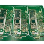
High-Frequency PCB and Microwave PCB: Where the Line Is
The two terms are used interchangeably in conversation and they describe overlapping sets of boards. A high-frequency board operates where the interconnect must be treated as a transmission line; a microwave board operates where the wavelength is short enough that distributed effects dominate the design entirely.
The difference is one of degree rather than of kind, and where the boundary is drawn depends on the design. What matters is that the requirements become more demanding as the frequency rises, and the process and the material have to keep up.
What the Terms Describe
A high-frequency board usually means a digital or mixed design whose clock or carrier frequency is high enough that impedance control, loss and skew have to be managed explicitly. It is a description of the design task rather than of the frequency band.
A microwave board usually means an analogue design at a frequency where the physical dimensions of the circuit are comparable to the wavelength. At ten gigahertz, a wavelength in a laminate is roughly fifteen millimetres, so a trace of a few millimetres is a significant fraction of a wavelength.
Frequency Ranges and Behaviour
Below a few hundred megahertz, a trace can often be treated as a lumped connection, and the design is dominated by resistance and by return path continuity. Above roughly a gigahertz, the transmission line behaviour has to be designed rather than checked.
Above ten gigahertz, the distributed nature of the circuit matters: a stub of a few millimetres resonates, a bend radiates, and a launch from a connector to a trace is a designed transition rather than a connection. That is the region where the term microwave is usually applied.
Material Selection
The loss budget drives the material. A high-frequency digital board often uses a mid-loss or low-loss laminate with a controlled dielectric constant, while a microwave board uses a material with a very low dissipation factor and a dielectric constant that is stable with frequency and temperature.
The copper foil matters more as the frequency rises, because the current crowds into the surface. A smooth, low profile foil reduces conductor loss, and on a microwave board the foil type is part of the specification rather than a detail left to the fabricator.
Transmission Line Structures
A high-frequency digital board uses microstrip, stripline and differential pairs, designed for a target impedance and for length matching. The structures are usually planar and the design rules come from the stackup.
A microwave board uses the same elemental structures but also uses them as circuit elements. A quarter wave stub is a filter, a coupled line is a directional coupler, and the physical length of a trace is part of the electrical function. The tolerance on the line width becomes a tolerance on the centre frequency.
Tolerances and Fabrication
Both rely on controlled impedance, which means the stackup, the line width and the dielectric thickness are specified and verified with a coupon. On a microwave board the additional requirements are the dimensional tolerance of the patterns that define a resonant structure and the consistency of the dielectric constant across the panel.
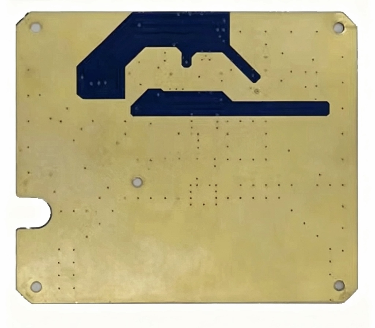
Surface finish, plating thickness and solder mask all affect the electrical behaviour of a microwave structure more than they affect a digital one, because they sit directly in the field of the line. A mask over a filter changes its centre frequency, which is why microwave boards are frequently supplied without mask over the critical structures.
Measurement and Verification
A high-frequency digital board is verified by an impedance coupon and by a time domain measurement of the channel. A microwave board is verified with a vector network analyser, measuring the scattering parameters of a test structure on the same panel.
The test structure is designed as part of the circuit rather than added afterwards. A thru, a line and a reflect standard for calibration are placed on the panel, and the measurement describes the process as it was applied to the product rather than as it was specified.
Where the Boundary Sits
In practice the boundary is a matter of design effort rather than of a specific number. A board at three gigahertz with a long channel and a tight loss budget needs the same discipline as a microwave board, while a board at twenty gigahertz with a very short connection may need less.
The useful question is whether the physical dimensions are a significant fraction of the wavelength and whether the loss and the impedance tolerance are part of the specification. Where both are true, the board is a microwave board whatever the product is called.
Design Checklist
Confirm the loss budget and the impedance tolerance before choosing the material, model the transitions rather than assuming them, specify the foil and the mask treatment for the critical structures and include a test coupon that describes the process.
gopcb builds high-frequency and microwave boards with low loss laminates, smooth copper foil, coupon based impedance verification and the surface finish control that a distributed circuit requires.
Connectors and Launches
The transition from a connector or a cable to the board is often the weakest part of a microwave circuit. The connector vendor provides a model of the launch, and the board footprint has to reproduce it: the pad size, the ground via placement and the layer on which the signal leaves the connector all affect the impedance through the transition. A footprint copied from a similar design rarely matches the model, and the mismatch appears as a reflection that no amount of tuning elsewhere will remove.
The mechanical interface matters as much as the electrical one. A connector that is anchored only by its signal pins will move under cable torque, and a movement of a fraction of a millimetre changes the launch geometry. The ground pins, the mounting screws and the board edge are all part of the transition, and they are specified together rather than as separate mechanical and electrical items.
Cost and Process Trade-offs
The cost of a high-frequency board rises with the material, the layer count, the tolerance and the inspection. The cheapest way to meet a given budget is usually to keep the highest frequency section as small as possible and to use a conventional material elsewhere in a mixed stackup, accepting the transition between the two as a designed element.
The number of process steps is the other driver. A board with back drilling, a filled via array and a fine line pattern costs more than one with none of those, so each of them is justified against the electrical requirement rather than applied by habit. Where a stub is short enough that its resonance is above the band of interest, back drilling adds cost without adding performance, and the design should demonstrate that before specifying it.
FAQ
Is a high-frequency PCB always a microwave PCB? No. A digital board at a few gigahertz is a high-frequency board, but its traces are short compared with the wavelength and its function is not distributed.
Does solder mask affect a microwave circuit? It does. The mask changes the effective dielectric constant above the line, which shifts the frequency of a resonant structure, so critical areas are often left unmasked.
Which material is used for microwave boards? A low loss laminate with a stable dielectric constant, often a filled or reinforced fluoropolymer, chosen from the loss budget rather than from a preference.
Related reading: high frequency laminate selection, microstrip and stripline routing, PTFE and ceramic substrates, and impedance discontinuity analysis.