Reading a Circuit Diagram and Tracing It onto a PCB
A circuit diagram is the description of a design, and a printed circuit board is the same design expressed in copper and laminate. Reading one means recovering the intent behind the drawing, and tracing it onto the board means checking that the intent survived. Both are learned skills rather than talents, and both follow a method that keeps the number of things you have to hold in your head at once to a minimum.
Classifications Worth Knowing
Before reading any particular drawing it is worth knowing what kind of board you are looking at, because the classification tells you what the layout can and cannot do. By layer count, boards are single sided, double sided, or multilayer with three or more conductor layers separated by insulating material and laminated together. A single sided board carries components on one face and conductors on the other, which makes it simple and inexpensive but unsuitable for a complex product. A double sided board has copper and routing on both faces, connected through plated holes. A multilayer board is the form that high speed, high density and high pin count products take.
By mechanical character, boards divide into rigid boards, flexible circuits, and rigid flex constructions that combine the two. A flexible circuit is built on a polyimide or polyester film and is characterised by high wiring density, light weight, thin construction and the ability to bend. Where a rigid circuit and a flexible one are laminated into a single part, the result is a rigid flex board carrying the properties of both, and the design rules of both apply to it. The families are described in PCB circuit board explained.

Start From the Outside
The method that works on almost any drawing is to work from the outside in. Begin at the edges of the diagram, where the components are the most recognisable: connectors, switches, sockets, power inputs, indicators. Those parts are physically large, their function is obvious from their shape, and their position in the diagram tells you which way the signals flow.
From each of those entry points, follow the connecting lines inwards. A connector leads to a protection component, then to a filter, then to an integrated circuit. That path is the signal path, and having established where the signal enters and where it is processed, the rest of the diagram becomes readable because the purpose of the intermediate parts is now clear.
Use the Integrated Circuits as Landmarks
Every diagram has weak points, and they are the places where reading becomes easy. Integrated circuits are the most useful of these, because their pin count and their position make them visually obvious, and because their function is generally known from the part number. A large device in the centre of a drawing is usually the processor or the controller, and the circuits around it are its support functions.
Once such a device is identified, the surrounding parts can be grouped by which pin they connect to. Components on the supply pins are decoupling. Components on the oscillator pins are the timing circuit. Components on the interface pins are the connections to the outside world. Reading outward from the device in that way converts a mass of symbols into a set of functional blocks.
Signal Flow and Return
Every signal has a source and a destination, and every one has a return path. In the diagram the return is drawn as a ground symbol, which hides the fact that the physical path matters. On the board the return current flows through copper, and where that copper is narrow or broken the circuit behaves differently from the drawing.
A reader who keeps that in mind will notice the things drawings tend to obscure: where a ground symbol appears at several places that are physically far apart on the board, where a signal crosses from one ground region to another, and where a return path is shared by circuits that switch at different rates. Those are the locations where a board that matches its diagram perfectly can still fail. Reading a diagram with that in mind is what separates a circuit that is understood from one that is merely copied, because the drawing describes intent and the board has to be checked against that intent rather than against the symbols alone.

From Diagram to Board
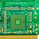
Reading a diagram and reading a board are two views of the same design, and comparing them is how a layout is checked. The trace in the drawing becomes a copper conductor, and the width of that conductor should follow the current it carries and the impedance it has to present. Where the diagram shows a shielded or twisted connection, the board shows a ground plane beneath the trace or a ground trace beside it.
The layer arrangement is the other half of the comparison. A four layer stack-up typically places signal, ground, power and signal in that order, so that each routing layer sits beside a plane. Understanding which layers carry what, and why, makes it possible to follow a signal from one side of the board to the other by following the vias. The arrangements used for different layer counts are described in layer stackup from one to eight layers, and the discipline that connects the drawing to the finished board is covered in PCB design and fabrication.
Common Traps
Three traps catch most readers. The first is treating the ground symbol as a single node: on the board it may be several regions joined at one point, and a signal that crosses between them has a return path problem. The second is following the signal and ignoring the supply, because a circuit that is correct on paper can still behave badly if the supply reaches the device through a long narrow path. The third is assuming that a device’s pin functions are as expected, when the datasheet describes several possible configurations and the drawing does not say which one is used.
The habit that avoids all three is to trace a circuit twice, once as a signal and once as a current loop, from source through the load and back to the source. A design that makes sense both ways is one that will behave on the board as it does on the drawing.
FAQ
Where should reading a circuit diagram start? At the outside, with the connectors, switches and power inputs, and then follow the connections inwards. Those parts are the most recognisable and they establish which way the signals flow.
Why are integrated circuits useful landmarks? Because a large device is visually obvious and its function is usually known from its part number. Components can then be grouped by the pin they connect to, which reveals the support circuits around it.
What is the most common mistake when reading a layout? Treating the ground symbol as one node. On the board it may be several regions joined at a single point, and a signal crossing between them has a return path that is not what the diagram suggests.
Why check the current path as well as the signal path? Because a circuit that is correct as a signal path can still fail as a current loop. Both views have to make sense for the board to behave as the drawing intends.