PCB Design Principles for a Reliable Layout
A correct schematic is not enough. A board built from a correct schematic can still be unreliable if the parts are arranged so that one circuit disturbs another, if the heavy components are unsupported, or if the outline leaves no room for the tooling that will hold the board.
This article sets out the principles that PCB design follows to avoid those outcomes, covering board size, the placement of special components, and the anti-interference rules that the arrangement of the functional blocks has to satisfy. None of the rules is difficult on its own; the difficulty is that they interact with each other.
Board Size: A Trade-Off in Both Directions
Board size is not simply a matter of fitting the circuit in. A large board gives long traces, which raises impedance, weakens noise immunity and increases cost, while a board that is too small has less area to dissipate heat and places adjacent traces close enough to interfere with each other.
The practical approach is to fix the size from the mechanical requirement, then place the special components, and only then distribute the rest of the circuit by functional unit. The size becomes a constraint that the placement works within rather than a quantity that the layout discovers at the end. Where the enclosure is fixed, the question is not how large the board can be but what the available area will hold.
Placing the Special Components First
The parts that have a requirement beyond their electrical function are placed before everything else. Devices that work at high frequency are placed close together so that the connections between them are short and the distributed parameters and coupling between them are small. Sensitive parts are kept apart from each other rather than clustered, and the input and output elements of a circuit are separated as far as the board permits.
The rest of the circuit then arranges itself around these constraints, which is the same order that produces a routable layout. The sequence used to place components is the mechanism, and the reason for the order is that some parts cannot be moved later.
High Voltage and Clearance
Where a potential difference exists between two conductors, the spacing between them has to be large enough that no discharge can occur, and the requirement grows with the voltage and with altitude or humidity. A high voltage section is also placed where a hand is unlikely to reach during debugging, which is a safety requirement rather than a performance one.
Clearance is not the only consideration: a slot milled through the board is sometimes used to increase the creepage path, and the components themselves have to be rated for the voltage they will see. The design rules that keep a layout efficient give way here to the safety rules, which take precedence.
Weight, Support and Heat
A heavy component cannot rely on its own leads. Anything above a modest mass is supported by a bracket or a strap and then soldered, and the very large parts, such as transformers, are usually mounted to the chassis rather than carried by the board at all.
Parts that generate heat are separated from the parts that measure it, and the arrangement of the heavy and the hot items tends to be decided together because both prefer the same place: the supported edge of the board. The behaviour of the board under that combination of mass and temperature is described under dimensional stability.
<img src="https://www.gopcba.com/wp-content/uploads/2026/08/Common_High_Frequency_PCB_Design_Mistakes.jpg.webp" alt="PCB layout arranged in functional blocks along the signal flow” />
Adjustable Parts and Enclosure Requirements
Parts that a person has to adjust are placed according to where the adjustment happens. If a trimmer is intended to be set with the board in place, it goes where a tool can reach it without disturbing anything else. If it is set from outside the case, then the position on the board has to line up with the opening in the panel, and the alignment is a mechanical dimension rather than a layout preference.
The same applies to switches, sockets and connectors. Each of them has a mechanical relationship with the enclosure, and the position of the part on the board is derived from that relationship. Places reserved for mounting holes and brackets are also fixed at this stage, and the outline and mounting features are what the placement has to respect.
Arranging the Functional Blocks
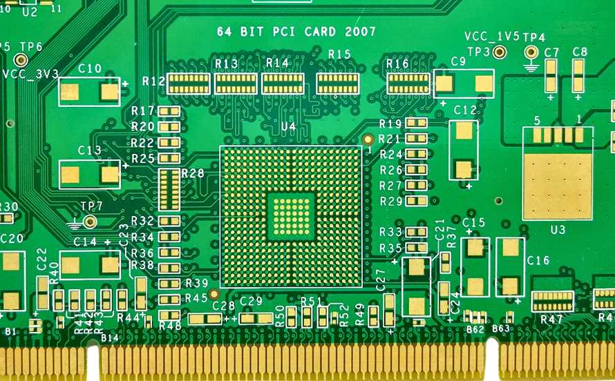
The circuit is divided into functional units, and each unit is arranged around its central device. The flow through the units follows the signal path, so that the parts of the circuit that exchange signals are adjacent and the connections between them are short and take the same general direction rather than doubling back across the board.
Within a unit, the parts are placed evenly and in a consistent orientation. That is not only a matter of appearance: a regular arrangement is easier to assemble, easier to inspect and easier to read, and on a high-frequency board the consistent orientation also helps to keep the coupling between traces predictable.
Interference: Direction, Parallelism and Spacing
Interference in a layout comes from three sources: traces that run parallel and couple into each other, currents that share a return path, and fields that a high-voltage or high-current circuit radiates into a sensitive one. The arrangement of the blocks addresses all three at once.
Signals are grouped by domain and each group is routed in its own direction, with high frequency separated from low frequency and analogue from digital. Where two groups must pass each other, the crossing is made at an angle rather than in parallel, and a grounded trace between them acts as a barrier. The reasoning behind the separation is set out in the mixed-signal layout guidelines.
Edge Clearance, Shape and Mechanical Limits
Components are kept a couple of millimetres clear of the board edge, because the profiling operation has a tolerance and because the edge is where handling damage occurs. A rectangular outline with an aspect ratio of roughly three to two or four to three is the most efficient shape to panelise, which reduces cost.
Beyond a certain size, the mechanical strength of the board becomes a design consideration in its own right, because a large panel that is handled and processed will flex. Where the outline is large, support points, stiffeners or a heavier construction have to be considered, and the rules for the outline apply to the shape as well as to the features placed on it.
FAQ
Should the circuit be split into small boards to avoid a large one? Only where the product allows it, since a split introduces connectors and cables that bring their own problems. A single board with a well organised layout is usually the better answer.
How is interference between two functional blocks prevented? By separating them in placement, by routing them in different directions, and by keeping their return currents apart. Distance is the first line and ground routing is the second.
Is an odd board shape a problem? It costs more, because the panel has to be arranged around it and material is wasted. Where the enclosure demands the shape, the cost is accepted rather than avoided. The shape carries a price, and it is better to know that price before the panel is arranged around it.