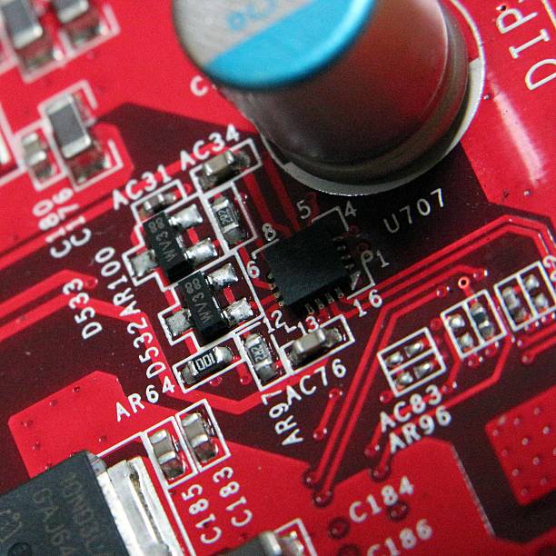
How to Solve EMI Problems in Multilayer PCB Design Electromagnetic interference rarely starts at the test chamber. Most EMI trouble in multilayer boards begins with a return current that cannot find a short path home. A split plane, a distant via, or a poorly coupled power pair turns a clean…
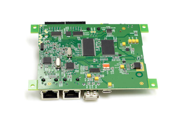
14 Key Characteristics of a High-Reliability PCB Two boards can share the same Gerber files and still behave very differently in the field. The gap sits in details that never appear on the drawing: hole-wall copper, residue on the surface, laminate tolerance, and the discipline behind each process step. A…
Best 6-Layer PCB Stackup for High-Speed Boards Six copper layers give a designer more room than four, and less cost than eight. That middle position explains why the six-layer board appears in embedded systems, industrial controllers and communication equipment. For high-speed work, the layer count alone decides very little. The…
How to Output Gerber Files Correctly for PCB Builds A finished layout is not yet a manufacturing package. The design must be converted into data a fabricator can read without your CAD seat. Gerber files carry the copper, mask, silkscreen and outline images. NC Drill files carry the hole positions…
How to Export PADS Gerber Files for Reliable PCB Builds Gerber data is the language a fabricator reads. If the export is wrong, the board is wrong, even when the layout itself is perfect. PADS handles this job through its CAM output tools, and the workflow is short once you…
Multilayer PCB Impedance Routing for Differential Pairs Differential pairs carry the high-speed traffic on most multilayer boards. A USB link, a display interface or a serializer lane all depend on two traces behaving as one controlled structure. Impedance routing is the discipline that keeps that structure intact from the driver…
Via-to-Trace Spacing in Multilayer PCB Design Vias connect signals between layers, and their placement shapes what the fabricator can build. When routing density rises, vias crowd together and move closer to traces and copper pours. A clearance that looks fine in CAD may sit below what the drill, plating and…
What Is a High-Reliability PCB? Reliability Explained A high-reliability PCB keeps its designed function across its full service life. It must survive electrical, thermal, mechanical and environmental stress without drifting outside specification. Passing a bare-board electrical test is not enough. The board must also support later assembly and stay stable…
Why High-Reliability PCB Manufacturing Matters A PCB that fails in the field costs far more than the board itself. Rework, warranty claims, downtime and lost reputation all trace back to process decisions made long before shipment. High-reliability manufacturing treats those decisions as engineering problems, not as luck. The goal is…
High-Current PCB Design: How to Prevent Board Burnout A board that burns out under load rarely fails without warning. The damage usually starts with a trace running too hot, a via carrying more current than it can handle, or a solder joint that slowly weakens under thermal cycling. High-current designs…