KingdaKingdaKingda

Call Us 24/7

+86-181-2376-9076

Send Us Mail

sales@gopcba.com

Our Location

Baoan District, Shenzhen, China

Language

  • enEnglish
    • fr France
    • itItalian
Kingda
  • Home
  • PCB Assembly
    • Prototype PCB Assembly
    • Turnkey PCB Assembly
    • Low Volume PCB Assembly
    • High Volume PCB Assembly
    • SMT PCB Assembly
    • Through Hole PCB Assembly
    • Mixed Technology PCB Assembly
    • Flex PCB Assembly
  • Services
    • PCB Design/Layout
    • PCB Manufacturing
    • Rapid PCBA Prototyping
    • Components Procurement
    • Conformal Coating
    • PCBA Testing
    • Box Build Assembly
    • Wire & Cable Harness Assembly
  • Industry Solutions
    • Medical PCBA
    • Telecommunications PCBA
    • Energy PCBA
    • Industrial PCBA
    • Artificial Intelligence PCBA
    • IOT PCBA
  • Resources
    • PCB Capabilities
    • PCBA Capabilities
    • FAQ
    • Blog
  • About Us
    • About Us
    • Why Us
    • Quality Management
    • Our PCB Assembly Process
  • Contact Us
Get A Quote
Rigid-Flex PCB

PCB Plated Hole Copper Thickness: Causes of PCB Failure

  • By 杰夫
  • 2026年 9月 6日
  • PCB Assembly
  • No Comments
PCB Plated Hole Copper Thickness: Causes of PCB Failure A board can pass continuity testing and still fail in the field. The hidden cause is often thin copper on the wall of a plated hole. Plated holes carry current between layers, and they also absorb thermal and mechanical stress. When…
Continue Reading
lead-free soldering

IPC Class 2 vs Class 3 PCB: Key Differences and Standards

  • By 杰夫
  • 2026年 9月 6日
  • PCB Assembly
  • No Comments
IPC Class 2 vs Class 3 PCB: Key Differences and Standards Two boards can leave the same shop with identical copper and still be judged by different rules. The IPC class decides which acceptance limits apply to holes, solder joints and surface features. It also shapes how much process control…
Continue Reading
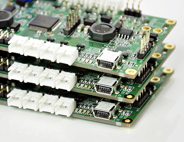
A stack of assembled PCBs on-top of each other, with narrow focus at the front.

Pseudo 8-Layer PCB: Structure and Manufacturing Explained

  • By 杰夫
  • 2026年 9月 6日
  • PCB Assembly
  • No Comments
Pseudo 8-Layer PCB: Structure and Manufacturing Explained A pseudo 8-layer PCB looks like an eight-layer board in the stackup drawing. It routes signals on only six copper layers. The extra copper-clad core sits in the middle of the structure, and its copper is etched away completely. The board therefore carries…
Continue Reading
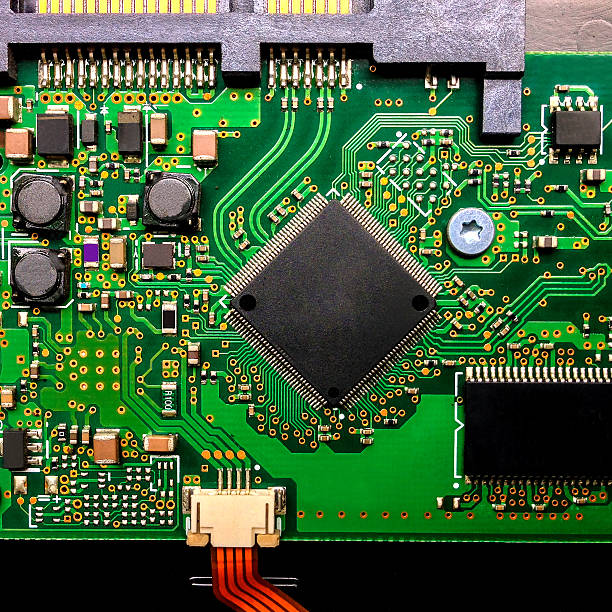
Circuit board from hard disc storage

PCB and PCBA Design Review Checklist for DFM and DFA

  • By 杰夫
  • 2026年 9月 6日
  • PCB Assembly
  • No Comments
PCB and PCBA Design Review Checklist for DFM and DFA A correct schematic does not guarantee a buildable board. Many failures appear only at fabrication or assembly, when a footprint disagrees with the BOM or a pad is too small. A structured design review catches these problems while changes are…
Continue Reading
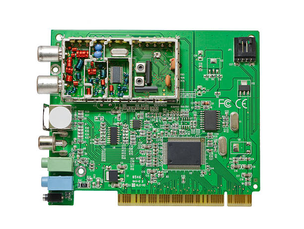
The internal TV tuner isolated on the white background

Single-Layer vs. Double-Sided vs. Multilayer FPC: Key Differences

  • By 杰夫
  • 2026年 9月 6日
  • PCB Assembly
  • No Comments
Single-Layer vs. Double-Sided vs. Multilayer FPC: Key Differences Flexible circuits carry a simple promise: connect components and route signals through a shape that bends. The layer count decides how much routing that shape can hold. A single copper layer suits simple interconnections. A double-sided build adds a second plane and…
Continue Reading
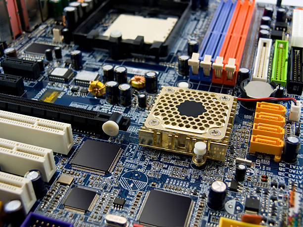
Close-up photo of view of system board (computer part)

PCB Panelization: 10 Critical Design Considerations

  • By 杰夫
  • 2026年 9月 6日
  • PCB Assembly
  • No Comments
PCB Panelization: 10 Critical Design Considerations Small boards are hard to hold, feed, and print. Panelization solves that by grouping several boards into one larger manufacturing format. The panel then travels through printing, placement, reflow, and inspection as a single unit. Good panel design keeps that unit rigid, aligned, and…
Continue Reading
22

PCB Right-Angle Routing: 3 Reasons to Avoid 90° Traces

  • By 杰夫
  • 2026年 9月 6日
  • PCB Assembly
  • No Comments
PCB Right-Angle Routing: 3 Reasons to Avoid 90° Traces A 90° corner looks harmless on a layout screen. It is quick to draw and easy to fit into tight spaces. Yet many experienced designers still steer around it whenever they can. The reason is not superstition or habit. A right-angle…
Continue Reading
Electronic device with blurred focus on white background

AOI Inspection in PCB Assembly: What It Checks

  • By 杰夫
  • 2026年 9月 6日
  • PCB Assembly
  • No Comments
AOI Inspection in PCB Assembly: What It Checks Automated optical inspection uses cameras to compare a finished board against a known good reference. The system captures images, analyzes them, and flags anything that falls outside the programmed limits. AOI is fast, repeatable, and non-contact, which makes it a natural fit…
Continue Reading
A printed circuit board with various electronic devices mounted on it.

PCB Gold Fingers: Complete Design and Manufacturing

  • By 杰夫
  • 2026年 9月 6日
  • PCB Assembly
  • No Comments
PCB Gold Fingers: Complete Design and Manufacturing Gold fingers are the exposed contacts along a board edge that mate with a slot or connector. They carry power and signals into memory modules, graphics cards and control boards. Because the same contacts slide in and out many times, they must be…
Continue Reading
PCB assembly lead time

PCB Hole and Slot Design: Mistakes to Avoid

  • By 杰夫
  • 2026年 9月 6日
  • PCB Assembly
  • No Comments
PCB Hole and Slot Design: Mistakes to Avoid Holes and slots look simple on a layout, yet they carry electrical, mechanical and assembly duties at the same time. A single wrong attribute can remove a pad, cover a mounting area, or leave a connector opening uncut. Most of these errors…
Continue Reading
1 … 1,528 1,529 1,530 … 1,621

Search Posts

Categories

  • Electronic Materials
  • Electronical Engineering
  • Industrial Control
  • PCB Assembly
  • PCB Design
  • PCB Manufacturing

Recent Posts

Low-Temperature Solder for LED Modules: Thermal Budget and Joint Reliability

Frank guo - 2026年 11月 6日
Surface Mount Technology (SMT): Process, Components, Design Guidelines & PCB Assembly

Surface Mount Technology (SMT): Process, Components, Design Guidelines & PCB Assembly

Zane Zhang - 2026年 10月 2日
Cheap PCB Costs: PCB Design, PCB Manufacturing & SMT vs TH Guide

Cheap PCB Costs: PCB Design, PCB Manufacturing & SMT vs TH Guide

Jelly - 2026年 9月 30日

Tags

AOI inspection automotive electronics automotive PCBA quality automotive standards box build assembly component procurement component supplier conformal coating defect prevention DFM checks DFM review e-bom management electronic component shortage electronic manufacturing services electronic manufacturing standards Electronic Materials electronics design best practice electronics manufacturing capacity electronics sourcing high volume production industrial electronics manufacturability review mass production quality mixed technology PCB PCBA inspection PCBA prototype PCBA turnkey PCBA volume pricing PCB Design PCB layout rules PCB Manufacturing PCB sourcing power electronics PCB printed circuit board prototype quick turn PCB reflow soldering reflow soldering profile SMT assembly quality SMT production soldering defect analysis solder joint quality solder paste inspection solder paste printing surface mount technology vehicle electronics
GOPCBA-logo

As a professional China PCB assembly manufacturer, we provide a full range of electronic manufacturing services from PCB fabrication, PCBA to OEM/ODM, including PCB design, PCB layout, rapid PCBA prototyping, components procurement, SMT/ THT assembly, china pcb assembly, china pcb prototype, PCBA testing and box build assembly.

Linkedin Facebook-f X-twitter Youtube Instagram

PCB ASSEMBLY

  • Prototype PCB Assembly
  • Low Volume PCB Assembly
  • High Volume PCB Assembly
  • Turnkey PCB Assembly
  • SMT PCB Assembly
  • Through Hole PCB Assembly
  • Mixed Technology PCB Assembly
  • Flex PCB Assembly

OUR SERVICES

  • PCB Design/Layout
  • PCB Manufacturing
  • Rapid PCBA Prototyping
  • Components Procurement
  • Conformal Coating
  • PCBA Testing
  • Box Build Assembly
  • Wire & Cable Harness Assembly

TECHNICAL SUPPORT

  • About Us
  • Quality Management
  • Artificial Intelligence PCBA
  • Industrial PCBA
  • IOT PCBA
  • Medical PCBA
  • Energy PCBA
  • Telecommunications PCBA

Copyright © 2026. Shenzhen Kingda Electronics Co., LTD  All rights reserved. 

  • Sitemap
  • Terms of Service
  • Privacy Policy
Zmdi Zmdi-email Phone-square Whatsapp Weixin
x

ABOUT US

Progressively maintain extensive infomediaries via extensible nich. Capitalize on low hanging fruit. a ballpark value added is activity to beta test. Override the digital divide with additional click throughs from fruit.

LOCATIONS

map

Shenzhen Office

+86-181-2376-9076
sales@gopcba.com
3rd Floor, Building 11, Houting Third Industrial Zone, Shajing Avenue, Baoan District, Shenzhen, China.
Contact Us

FOLLOW US