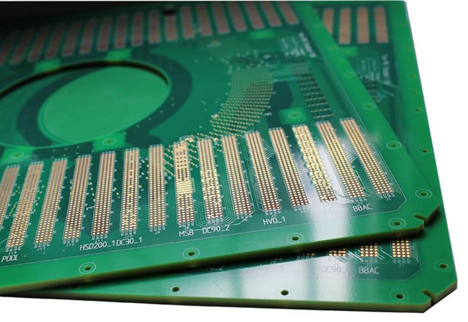
2026 Hybrid Multilayer PCB Cost Guide – Latest Pricing & Key Factors With the rapid growth of AI servers, 800G/1.6T switches, 5G base stations, automotive millimeter-wave radar, satellite communications, and high-speed data centers, hybrid multilayer PCBs have become the mainstream solution for high-frequency, high-speed electronic designs. Compared to traditional FR4…
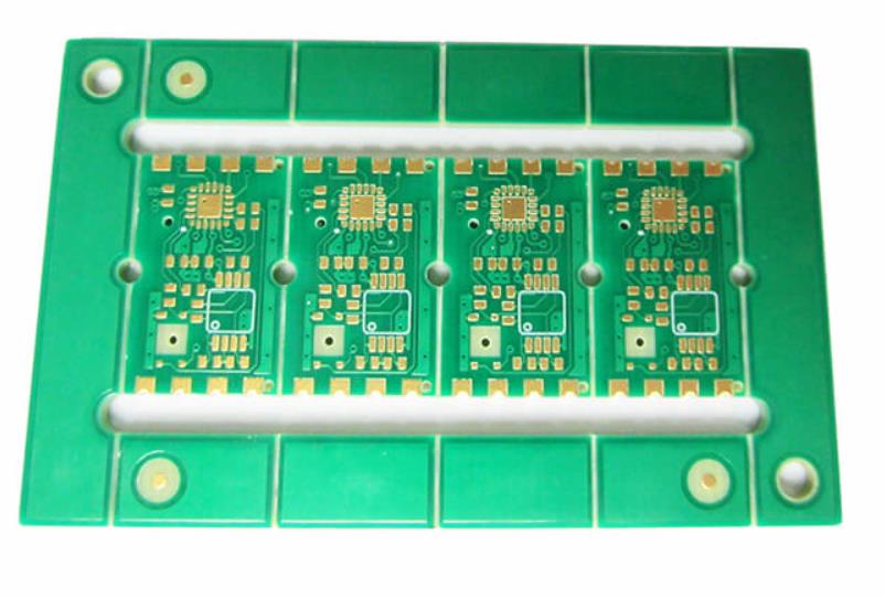
Castellation PCB Cost Analysis 2026 – How Materials, Layer Count & Process Affect Pricing With the rapid growth of IoT, wireless communication modules, smart home devices, medical electronics, and industrial control equipment, castellation PCBs (also known as stamp-hole or half-hole PCBs) have become a critical enabler for modular electronic products.…
FR4 vs Rogers PCB for RF Modules – Which Material Is Better for Your RF Product? With the rapid development of wireless technologies such as 5G, Wi-Fi 6/7, Bluetooth, LoRa, Zigbee, GPS, automotive millimeter-wave radar, and satellite communications, RF modules demand increasingly stringent PCB materials. For RF module design, the…
High Temperature PCB Manufacturing Process: Complete Guide from Material Selection to Final Testing With the rapid development of new energy vehicles, aerospace, industrial automation, petroleum exploration, military equipment, and high-power power supplies, electronic devices are increasingly required to operate stably for extended periods in high-temperature environments ranging from 150°C to…
High-Speed PCB and Six-Layer Stack-Up Design Choices A six-layer board can balance routing density, power delivery, and high-speed signal performance. Adding copper layers alone does not improve circuit behavior. The layer order, reference planes, dielectric spacing, and routing plan must work together. For fast interfaces, the stack-up decides whether return…
Multilayer PCB Impedance Routing: Differential Pair Design A differential pair carries one signal on two traces, and the receiver reads only the difference between them. That arrangement works because the two traces travel together through the same stackup, the same reference planes, and the same process window. When the geometry…
Multilayer PCB Via Spacing: Hole-to-Hole and Hole-to-Trace Design Via spacing is one of the quiet decisions that decides whether a multilayer board builds cleanly. Routing density gets the attention, but the gap between two drilled holes and the gap from a hole to nearby copper drive yield. A design that…
Pseudo 8-Layer PCB Structure: Design and Build Checks A pseudo 8-layer PCB is a six-layer board built with a stackup that resembles an eight-layer construction. The extra core carries no active copper circuitry. Instead, it thickens the dielectric between selected signal layers. Engineers use this trick when two signal layers…
Single-Sided vs Double-Sided vs Multilayer FPC: Key Differences A flexible printed circuit carries copper on a thin polymer film instead of a rigid board. The number of copper layers decides how much routing the part can hold and how it will behave when bent. Single-sided, double-sided and multilayer FPCs share…
PCB Panelization: 10 Key Design Considerations for Manufacturing Small boards are hard to handle on automated lines. Panelization groups several units into one rigid panel so printers, placers, and ovens can process them together. The panel is a manufacturing carrier, not a product, yet it decides how well the real…