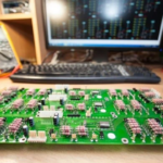


Introduction
When you invest in PCB assembly, the cost of failure is not just financial — it can damage your product reputation and delay time to market. A poorly tested circuit board may fail in the field, leading to returns, rework, or even safety risks.
That’s why PCB testing methods are a critical part of modern electronics manufacturing. A reliable PCB assembly manufacturer will implement multiple testing strategies to ensure quality, performance, and long-term reliability.
In this guide, we’ll walk through how to test a PCB, followed by the 7 most important PCB testing methods used in the industry today.
How to Test a PCB: Where to Start
If you’re wondering how to test a circuit board, the answer isn’t a single method. Effective testing is a layered validation process that typically includes:
1. Visual Inspection
The first step is identifying visible defects, either manually or through Automated Optical Inspection (AOI).
Common issues detected:
- Missing components
- Misalignment
- Solder bridges
- Surface defects
Catching these early prevents costly downstream failures.
2. Electrical Testing
Next, manufacturers verify electrical integrity to ensure the PCB matches the original design.
Typical methods:
- In-circuit testing (ICT)
- Flying probe testing
These tests detect opens, shorts, and incorrect component values.
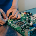
3. Functional Testing
Finally, the board is powered on to confirm it performs as intended in real-world conditions.
For high-reliability applications, additional stress testing such as burn-in testing may be required.
👉 In practice, PCB testing is not a single step — it’s a structured process designed to eliminate risk before shipment.
7 Types of PCB Testing Methods
Different testing methods serve different purposes. Most projects require a combination of tests to balance cost, speed, and coverage.
1. In-Circuit Testing (ICT)
In-circuit testing is one of the most comprehensive PCB testing methods available.
- Uses a bed-of-nails fixture to contact test points on the PCB
- Checks electrical performance of individual components
- Detects shorts, opens, and solder issues
- Coverage typically reaches 85–90%
Best for:
- High-volume production
- Mature designs with minimal revisions
Consideration:
Requires dedicated fixtures and must be planned during the PCB design stage.
2. Flying Probe Testing
Flying probe testing is a flexible and cost-effective alternative to ICT.
- Uses moving probes instead of fixed fixtures
- Tests opens, shorts, resistance, capacitance, and more
- No custom fixture required
Best for:
- Low- to medium-volume production
- Prototyping and early-stage designs
Limitation:
Slower than ICT and does not power up the board.
3. Automated Optical Inspection (AOI)
AOI testing uses high-resolution cameras to inspect PCB assemblies.
- Compares actual board images with design data
- Detects placement errors and solder defects
- Can be 2D or 3D inspection
Best for:
- Early defect detection
- Inline production quality control
Important:
AOI should be combined with electrical or functional testing for full coverage.
4. Burn-In Testing
Burn-in testing is a stress test designed to identify early-life failures.
- Runs the PCB under maximum load conditions
- Typically lasts 48–168 hours
- Identifies “infant mortality” failures
Best for:
- Medical, military, and high-reliability products
Consideration:
Can reduce product lifespan if over-applied.
5. X-Ray Inspection (AXI)
X-ray inspection is essential for modern high-density PCB designs.
- Detects hidden solder joints (e.g., BGA, QFN packages)
- Identifies internal defects and voids
- Available in 2D and 3D
Best for:
- Complex, multilayer PCBs
- High-density assemblies
Limitation:
Requires skilled operators and adds cost.
6. Functional Testing
Functional testing verifies that the PCB works in its actual application environment.
- Simulates real operating conditions
- Confirms full system performance
- May require custom fixtures and test setups
Best for:
- Final product validation
- Ensuring performance before shipment
7. Other Specialized PCB Tests
Depending on your application, additional PCB testing services may include:
- Solderability testing – Ensures reliable solder joints
- Contamination testing – Detects ionic residues causing corrosion
- Micro-section analysis – Examines internal structure defects
- TDR testing – Identifies issues in high-frequency circuits
- Peel testing – Measures laminate bonding strength
- Thermal stress testing – Evaluates heat resistance
These tests are often used in high-performance or mission-critical applications.
Choosing the Right PCB Testing Strategy
Not every PCB requires every test. The right combination depends on:
- Product complexity
- Production volume
- Reliability requirements
- Budget constraints
For example:
- Prototype stage → Flying probe + AOI
- Mass production → ICT + AOI
- High-reliability products → Functional + burn-in + X-ray
👉 The most effective approach is to work with a PCB assembly partner early in the design phase to ensure testability is built into the board.
Why PCB Testing Matters
Skipping or minimizing testing can lead to:
- Field failures
- Product recalls
- Increased warranty costs
- Damage to brand reputation
A well-defined PCB testing process ensures your product performs reliably from day one.
Looking for Reliable PCB Assembly and Testing Services?
Choosing the right partner is critical to ensuring product quality and consistency.
We offer:
- Full PCB assembly services (SMT & through-hole)
- Advanced PCB testing methods (ICT, AOI, X-ray, functional testing)
- Prototype to mass production support
- Design for manufacturability (DFM) assistance
👉 Contact us today to discuss your project and get a fast, competitive quote.