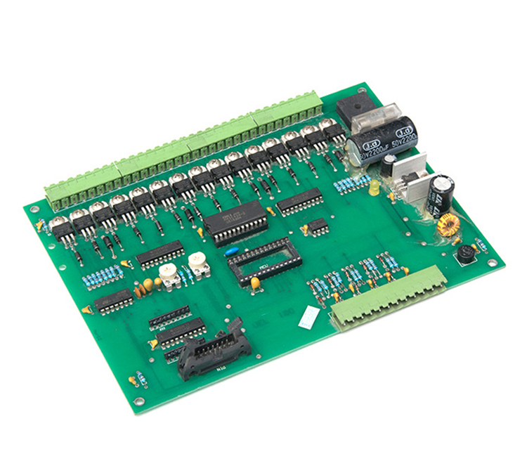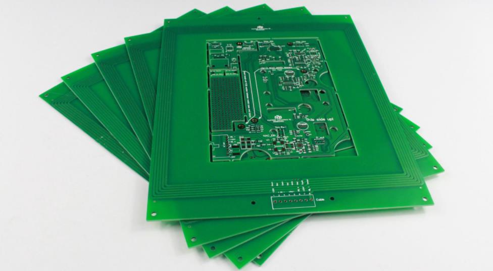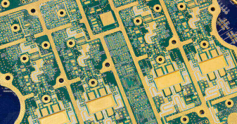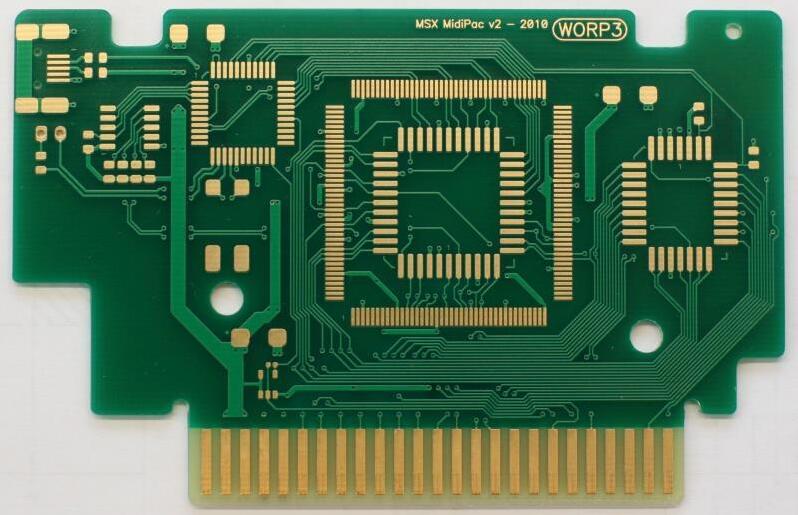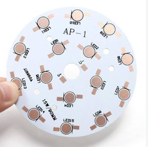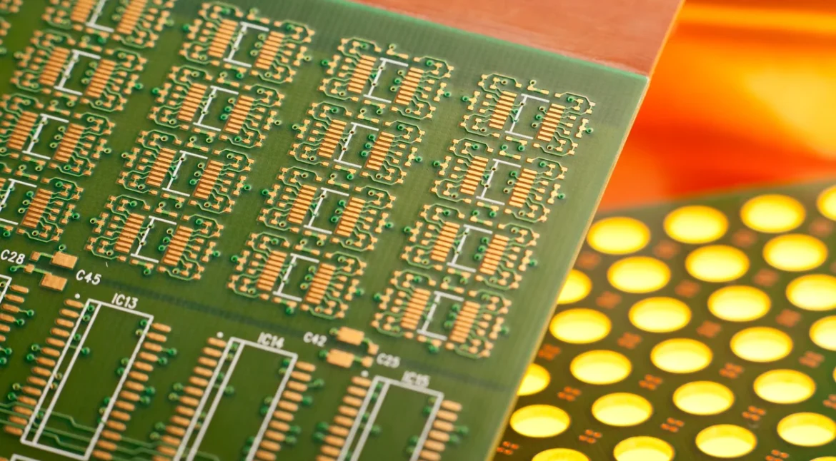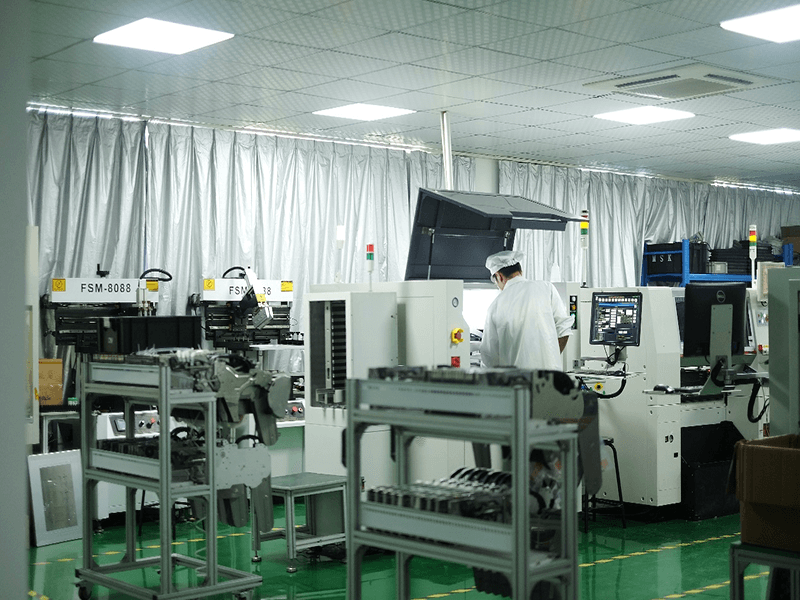
What Drives PCB Manufacturing Cost: Layers, Vias and Materials Layout effort goes into placement and routing, and the cost that the layout creates is usually noticed later, when the quotation arrives. Most of that cost is decided by a small number of choices, and almost all of them can be…
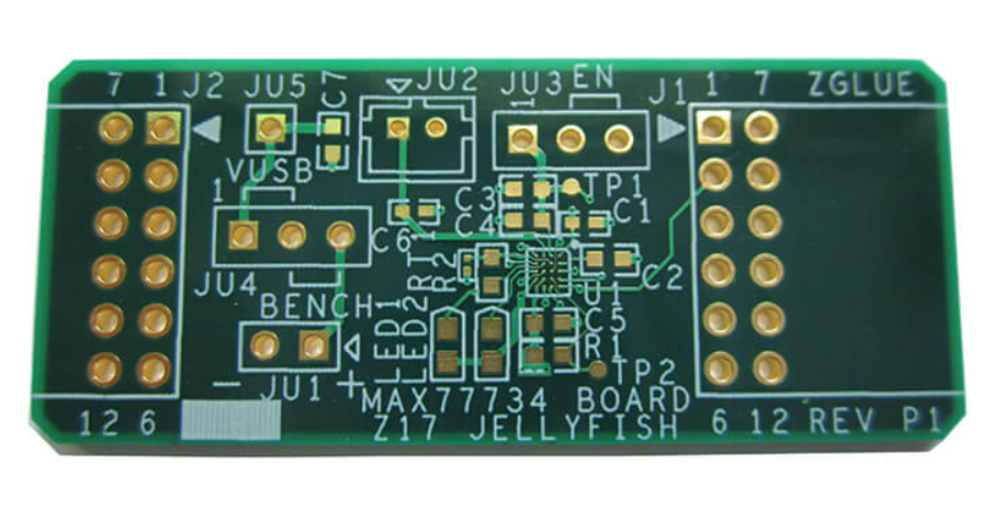
PCB Staking Material Selection: A Practical Review for Manufacturing Teams Buyers and engineers often focus on the finished product and forget the production line behind it. In practice, most field failures can be traced back to process decisions made during assembly. Understanding PCB staking material selection gives you a practical…
Panelization for Assembly: V-Cut, Tabs and Tooling Strips Surface mount lines handle panels, not single boards. A bare board that is 60 mm by 40 mm cannot be fed through a printer, a placer and a reflow oven on its own, so it is built as part of an array…
PCB Coating Thickness on Edges: The Hard Places to Cover Electronics manufacturing has become a discipline of small details. Solder paste volumes, placement accuracy, temperature profiles and inspection limits all add up to the final result. This guide looks at PCB coating thickness on edges from the perspective of a…
PCB Coating Pinhole Detection: From Prototype to Volume Production Electronics manufacturing has become a discipline of small details. Solder paste volumes, placement accuracy, temperature profiles and inspection limits all add up to the final result. This guide looks at PCB coating pinhole detection from the perspective of a PCBA factory…
Schematic Conversion Between Design Tools: What Breaks Designs change hands. A product line is acquired, a customer supplies an older board for a derivative, an engineering team consolidates onto one tool, or a design is taken over from an external developer who used something else. In each case a schematic…
PCB Coating Coverage Inspection: Key Process and Quality Checks Electronics manufacturing has become a discipline of small details. Solder paste volumes, placement accuracy, temperature profiles and inspection limits all add up to the final result. This guide looks at PCB coating coverage inspection from the perspective of a PCBA factory…
Repeated Module Placement in Multi-Channel PCB Layout Many boards are the same circuit repeated. An eight channel amplifier, a four port transceiver, an LED driver array or a bank of identical sensor front ends: the schematic describes one channel and the layout has to place and route it several times.…
PCB Corrosion Test for Coatings: A Factory-Floor Review Modern electronics depend on boards that are assembled correctly the first time. Every product – a phone, a charger, a medical instrument or an industrial controller – relies on thousands of solder joints that must conduct current for years. This article explains…
EMC Design Rules for High-Speed PCB Layout EMC problems are almost never solved by a component added at the end of a project. They are avoided by decisions taken at the start of the layout, when the placement, the stack-up and the routing of the critical nets are still open.…