PCB Blind Routing: Step Milling and Cavity Design
Most boards have a single thickness and a flat outline, and the milling that defines the shape goes all the way through. Blind routing changes that by removing material to a controlled depth, leaving a ledge, a recess or a cavity in the finished board. It is the process that allows a component to sit below the surface or a housing to close flush against the board.
What Blind Routing Produces
The process removes material from one or both faces without cutting through. The result may be a shallow recess that lets a tall component clear a lid, a ledge that supports a module, or a cavity deep enough to house an assembly below the board surface.
The term step milling is used for the same operation when the removal is arranged in stages, producing more than one depth in the same panel. Together they turn the board outline into a three dimensional feature rather than a two dimensional shape.
Why the Feature Is Used
The first reason is height. A product that has to be thin cannot always accommodate the tallest component, and a cavity lets that component sit inside the thickness of the board instead of on top of it, which removes its height from the stack up.
The second is mechanical. A recess can locate a module, hold a lens or an antenna at a defined distance from the board, or provide a pocket for potting compound. All of these are hard to achieve with a flat board and a bracket, and the routing replaces several parts with a single feature. The relationship with the outline as a whole is described in board outline and mounting design.
How the Depth Is Controlled
Controlled depth milling is performed with a router bit or an end mill set to a specific depth, using a machine with a depth reference taken from the panel surface. The reference matters, because the finished board thickness varies across the panel.
The achievable tolerance is what separates a routine job from a difficult one. A depth tolerance of plus or minus a tenth of a millimetre is straightforward, while plus or minus two hundredths requires a machine with accurate depth control, a flat panel and a process that accounts for the thickness variation of the laminate itself.

Remaining Thickness and Web Thickness
The material left under the cavity, known as the web, has to be thick enough to keep the board rigid and to hold the remaining layers intact. A web that is too thin flexes, cracks during handling or fails when the assembly is clamped.
The web thickness also has to be consistent with the layer stackup. If the cavity floor cuts into a layer that was intended to carry signals, those conductors are lost. The design drawing should state which layers remain under the cavity, and the routing depth should be derived from the stackup rather than from the finished board thickness alone.
Design Rules
The cavity should be positioned away from the board edge by a margin that leaves enough material for handling and for the routing tolerance. Corners inside the cavity should be rounded rather than square, since a router bit leaves a radius in any case and a square corner in the drawing becomes a negotiation at manufacturing.
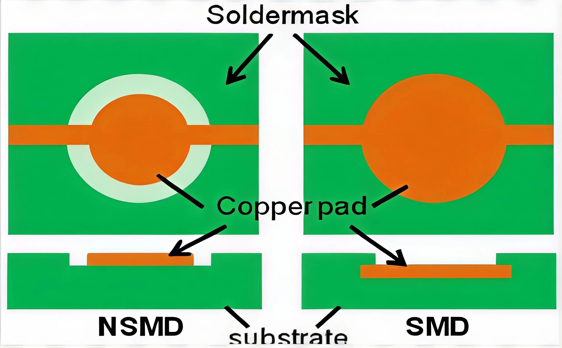
Copper in the cavity floor needs a clearance from the routed wall, because the milling tolerance can expose it. Where pads are placed inside a cavity, the solder mask and the finish have to be compatible with the process, and the assembly operation has to be able to reach the area. All of these details should be settled before the panel is designed, and the prototype considerations in multilayer PCB prototype requirements apply with more force than usual because the feature is expensive to change.
Effect on Assembly
A cavity changes the assembly process in several ways. Paste printing over a recess needs a stencil that can seal against an uneven surface, which usually means a step stencil or a separate printing operation. A cavity also traps flux and cleaning fluid unless there is a path for them to escape.
Where the cavity holds a module, the depth has to account for the adhesive or the solder that attaches it, and the tolerance stack has to leave the module at the correct height. Designing the cavity to the nominal dimension and relying on the process to absorb the variation is the usual cause of a module that sits proud of the surface.
Cost and Yield Considerations
Blind routing adds cost for three reasons. The machine time is longer than for a through cut, the operation is usually performed in more than one pass, and the risk of scrapping a board is higher because a depth error ruins a finished panel rather than an outline.
Yield falls as the tolerance tightens and as the web becomes thinner. Suppliers therefore price the feature according to the tolerance specified, and a drawing that states a tighter tolerance than the design needs pays for capability that is never used. Reviewing the tolerance requirement with the fabricator usually reduces both the price and the risk.
Interaction with the Stackup
Cavities are usually created after lamination, so the stackup has to be designed with the depth in mind. A build with an asymmetric stackup already wants to warp, and removing material from one face makes it worse, so a balanced construction is more important than on an ordinary board.
Where the cavity is deep, the remaining material may be only a few layers. That reduces stiffness and changes the thermal path, and it also affects the impedance of any controlled lines that pass under or beside the cavity. The general guidance in PCB design guidelines for manufacturability applies, with the additional instruction to keep critical radio frequency or high speed lines out of the cavity floor unless the geometry has been modelled with the reduced material present.
Inspection and Verification
Depth is verified by measurement rather than by eye, using a depth gauge or a coordinate measuring machine on a sample from each panel. A microsection shows the remaining layers and confirms that the web is intact and that no copper has been exposed.
The finished assembly should be checked with a height gauge or with the actual mating part. A cavity that is correct on the drawing and wrong when the lid is fitted is a tolerance stack problem, and the only reliable test is fitting the real components together rather than checking each dimension in isolation.
FAQ
Can any board have a routed cavity? Most multilayer boards can, provided the stackup leaves enough material and the design keeps the feature away from the edges. Thin boards are limited because there is not enough material to remove.
How deep can the routing go? To within a few layers of the opposite face, depending on the tolerance required. Deeper cavities need a thicker web and therefore a thicker board.
Does the cavity need a coating? The exposed laminate in a cavity can absorb moisture, so a coating or a sealed enclosure is worth considering where the product is exposed to humidity.