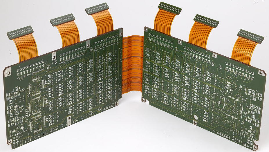
PCB Design Experience: Board Size, Decoupling and Heat
Most of what an experienced designer knows about layout is not theory; it is a set of habits that were learned from boards that behaved badly. The PCB design experience collected below covers the decisions that come up on nearly every project, with the numbers that make them concrete.
Board Size and Its Consequences
board size is a compromise with real electrical consequences. A board that is too large lengthens the traces, which raises impedance, increases susceptibility to noise and adds cost. A board that is too small concentrates the heat, crowds the routing and makes the coupling between adjacent lines worse. The useful target is the smallest board that still leaves room for a continuous ground plane and reasonable spacing between functional blocks.
Grouping Parts That Belong Together
Parts that work together should sit together. In particular, the clock generator, the crystal and the clock input of the processor should be close to each other, because the clock is the most likely source of radiated noise on the board and the most likely victim of it.
Devices that generate noise, low-current circuits and high-current circuits should all be kept away from the logic section. Where a high-current or high-noise block cannot be separated on the same board, the better answer is often a separate board, which is a decision worth making early rather than after the first EMC failure.
Decoupling Capacitor Practice
A decoupling capacitor is a local reservoir that supplies the transient current a device needs before the supply can respond. Placement matters more than value: the capacitor has to be connected to the pin and to ground with the shortest, widest connection the layout allows, and any inductance in that path makes the capacitor useless at the frequencies where it is needed.

The usual configuration is a bulk capacitor at the supply entry, in the range of 10 to 100 microfarads, and one small ceramic capacitor per integrated circuit, typically 0.01 to 0.1 microfarads. Where space does not allow a capacitor per device, a shared 1 to 10 microfarad capacitor can serve several devices, but the connection inductance grows with every device it serves. High-frequency bypass capacitors should not have long leads or long trace stubs, and where the supply enters through a connector, the bulk capacitor belongs right at that point.
Devices that are sensitive to supply variation, and memory devices whose current changes abruptly, should have their decoupling capacitor connected directly between the supply pin and the ground pin rather than somewhere along the net. Low cost signal quality improvements covers other measures that add little to the cost of the board.
Heat Dissipation and Board Orientation
heat dissipation improves when boards are mounted vertically rather than flat, because convection works with the designer instead of against them, and when a gap of at least 20 mm is left between adjacent boards in a stack. Where forced air is available, the airflow should be directed along the board rather than across it, so that each row of components is not preheated by the row in front of it.
Within the board, the arrangement of parts should follow a few rules. Place the dissipating components near the edges or near a mounting point where heat can leave through the chassis, keep temperature-sensitive parts upstream of the hot ones in the airflow, and do not place two dissipating parts side by side in a confined area.
Placement Order
Place the parts in the order that the constraints arrive. Mechanically fixed items come first: connectors, mounting holes, indicators and anything whose position is set by the enclosure. Then the large active devices, then the parts that must sit close to them, and finally the passives. Following this order avoids the situation where a connector has to be moved after the whole board has been laid out around it.
Then apply the separation rules to the result: high speed and low speed apart, analogue and digital apart, noise sources and sensitive receivers apart. These are easier to satisfy by moving whole blocks than by adjusting individual components. Copper flooding: mesh or solid covers how the remaining copper should be used to help.
What Experience Actually Buys
The difference between an experienced designer and a beginner is mostly in the order of work and in the willingness to move parts. An experienced designer will spend a disproportionate amount of time on placement, adjust it repeatedly as the routing reveals problems, and treat the router as a tool that executes a decision rather than one that makes it.
The other habit worth copying is documentation. A layout that records why a partition was made, which nets are critical, and what the impedance targets are can be picked up by another engineer without a conversation.
It is also worth keeping a record of what went wrong on previous projects. A short list of past layout mistakes, with the fix that worked, is more useful during a review than any checklist, because it is specific to the products the team actually builds.
Reviews Before Release
Measures That Cost Nothing
Several of the most effective layout habits add no cost to the board. Widening a power trace costs only area. Adding a ground via beside a layer change costs only a hole. Routing a sensitive trace on the layer next to a solid plane rather than on the surface costs nothing at all and improves the return path immediately. Keeping the switching node of a regulator small costs only the discipline of not drawing it large.
Others cost very little but require a decision. A dedicated ground plane on a two-layer board is impossible, but a ground grid with vias linking the top and bottom pours produces a measurable improvement for a small amount of routing area. A ferrite bead in series with a supply feeding a noisy block costs cents. Placing a slot between a heat source and a sensitive input costs a routed outline. These are the changes that rescue marginal designs, and they are much easier to make before the board is released than after.
A short review before releasing the board catches most of the expensive mistakes. Check the placement against the mechanical drawing, the decoupling against the device list, the critical nets against the impedance requirements and the plane structure against the current paths. Ask specifically whether anything on the board will be hot, whether anything is sensitive to temperature, and whether the two are neighbours.
The measures that most often rescue a marginal design are cheap ones: a wider trace, an extra ground via, a slot between a heat source and a sensitive block, or a second decoupling capacitor. EMI suppression design principles lists the layout techniques that make the most difference for the least effort.
FAQ
How small should a board be? As small as the design rules, the thermal load and the grounding requirements allow. Size is a consequence of the design, not a target to be set first.
Is a capacitor per chip really necessary? For any device with fast switching edges it is the cheapest reliability measure available. If space forces sharing, keep the shared capacitor close to the group and accept the reduced effectiveness.
Does board orientation really matter? For a passively cooled board it does. Vertical mounting and a gap between boards improve convection, and both are free if they are considered before the mechanical design is frozen.