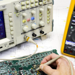
What Is PCB Design?
PCB Design is the process of converting an electronic circuit concept and schematic into a physical printed circuit board (PCB) that can be manufactured, assembled, tested, and used reliably in its intended application.
A PCB design integrates electrical circuits, component placement, copper routing, layer stackup, mechanical dimensions, thermal management, manufacturing requirements, and testing considerations into a single engineering solution.
Although PCB design may appear to be a straightforward process of connecting components with copper traces, modern boards can be highly complex. High-speed interfaces, dense component placement, power electronics, RF circuits, thermal constraints, miniaturization, and regulatory requirements all influence the final design.
A successful PCB Design must balance electrical performance, mechanical requirements, manufacturability, reliability, cost, and product requirements.
Modern products such as smartphones, laptops, wireless devices, automotive electronics, industrial controllers, medical equipment, and communication systems all rely on carefully engineered PCB designs.
A well-designed PCB can help the electronic circuit achieve its intended performance, while a poorly designed board may introduce signal noise, power instability, excessive heat, electromagnetic interference (EMI), manufacturing defects, or reliability problems.

Key Factors That Affect PCB Design
Several factors must be considered during the PCB Design Process. The relative importance of each factor depends on the application and product requirements.
Electrical Performance
Electrical performance is one of the most important aspects of PCB design.
Signal Integrity
Signal Integrity describes how accurately electrical signals propagate through their intended paths.
For high-speed designs, trace impedance, return paths, layer transitions, vias, crosstalk, reflections, transmission-line effects, and termination methods can significantly affect signal quality.
Poor signal-integrity design may result in:
- Signal reflections
- Crosstalk
- Overshoot and undershoot
- Timing errors
- Excessive electromagnetic radiation
- Data transmission failures
High-speed interfaces therefore require careful control of routing geometry, reference planes, stackup, and return-current paths.
Power Integrity
Power Integrity focuses on delivering stable power and return paths to components across the required frequency range.
A good power-distribution design considers:
- Power and ground planes
- Decoupling capacitors
- Current paths
- Voltage drop
- Plane impedance
- Transient current demand
- Via placement
- Power distribution network behavior
Poor power integrity can cause voltage fluctuations, excessive noise, component malfunction, and unwanted thermal stress.
Material Selection
PCB materials influence dielectric behavior, thermal performance, mechanical strength, and signal propagation.
Common materials include FR-4 for general-purpose applications, while high-frequency laminates, low-loss materials, high-Tg materials, flexible materials, and metal-core constructions may be selected for specialized applications.
Material selection should be based on electrical, thermal, mechanical, environmental, and manufacturing requirements rather than simply choosing the lowest-cost laminate.
Mechanical Requirements
Mechanical considerations are another important part of PCB Design.
Board Dimensions
PCB length and width must fit within the product enclosure while also satisfying mounting, connector, thermal, and assembly requirements.
Large or thin boards may be more susceptible to bending or mechanical deformation, particularly during assembly and handling.
Board Thickness
PCB thickness affects mechanical rigidity, impedance, thermal behavior, connector compatibility, and manufacturing considerations.
A thinner board may be useful where weight or space is limited, while a thicker board may provide greater rigidity. However, thickness should be selected according to the complete mechanical and electrical requirements.
Flexibility
Flexible PCBs use materials such as polyimide to support controlled bending.
Rigid PCBs, in contrast, are not intended to be repeatedly bent during normal operation unless the structure has been specifically designed for that purpose.
For rigid-flex or flexible designs, bend radius, copper thickness, layer count, stiffeners, bend direction, and dynamic versus static bending conditions should all be considered.
Additional Mechanical Factors
Other mechanical considerations include:
- Mounting-hole locations
- Connector positions
- Component height
- Keep-out areas
- Enclosure clearance
- Board edge requirements
- Heat-sink interfaces
- Fastening methods
- Panelization requirements
Economic Considerations
Cost should be considered from the beginning of the PCB Design Process, not only after the board is completed.
Important cost factors include:
- PCB layer count
- Board dimensions
- Material selection
- Copper thickness
- Minimum trace and spacing requirements
- Via technology
- Surface finish
- Component selection
- Assembly complexity
- Testing requirements
- Production volume
- Panel utilization
Advanced technologies such as HDI, microvias, fine-pitch routing, special laminates, and complex stackups can increase manufacturing cost.
However, simplifying a design only to reduce PCB cost can create other expenses through reduced performance, increased assembly difficulty, or reliability problems.
PCB Design Software and Engineering Tools
Modern PCB Design Software provides an integrated environment for schematic capture, component management, PCB layout, rule checking, documentation, and manufacturing data generation.
Common EDA platforms include Altium Designer, Cadence OrCAD/Allegro, Siemens Xpedition, KiCad, and other professional tools.
The appropriate software depends on design complexity, team requirements, existing workflows, and manufacturing data requirements.
Simulation and Analysis Tools
Simulation and analysis tools can help engineers identify potential electrical problems before physical prototypes are manufactured.
SPICE-based tools can be used for circuit simulation and analog or mixed-signal analysis.
For high-speed designs, specialized tools can evaluate:
- Signal Integrity
- Power Integrity
- Impedance
- Crosstalk
- Reflections
- Timing
- Electromagnetic behavior
These analyses are not necessarily required for every PCB. Simple low-speed designs may not require advanced simulation, while high-speed, RF, and complex power systems can benefit significantly from pre-layout and post-layout analysis.
Prototyping and Test Equipment
Prototype development is an important part of the PCB design cycle.
Depending on the application, engineers may use:
- Oscilloscopes
- Multimeters
- Logic analyzers
- Spectrum analyzers
- Network analyzers
- Programmers and debuggers
- Electronic loads
- Power supplies
- Thermal measurement equipment
Testing helps determine whether the physical board performs according to the original electrical and mechanical requirements.
PCB Design Process: From Concept to Production
A systematic PCB Design Process helps reduce design errors and improves communication between engineering, manufacturing, assembly, and testing teams.
1. Requirements and Concept Analysis
The process begins by defining the product requirements.
The specification should cover:
- Electrical requirements
- Mechanical dimensions
- Component requirements
- Operating voltage and current
- Signal-speed requirements
- Environmental conditions
- Thermal requirements
- Reliability targets
- Regulatory requirements
- Manufacturing constraints
- Target production volume
- Cost objectives
Clear requirements provide the foundation for later schematic and layout decisions.
2. Schematic Design
The schematic is the logical representation of the electronic circuit.
Engineers select components, define electrical connections, establish power domains, and verify circuit functionality.
At this stage, the Bill of Materials (BOM) and preliminary netlist can also be developed.
A schematic review should be completed before moving to detailed PCB layout.
3. Component Selection and Library Management
Component selection has a direct impact on PCB size, cost, thermal performance, assembly, and long-term product availability.
Engineers should consider:
- Electrical ratings
- Package type
- Tolerance
- Temperature range
- Power dissipation
- Lifecycle status
- Availability
- Approved alternatives
- Assembly requirements
Accurate PCB footprints and schematic symbols are equally important. An incorrect footprint can cause serious problems even when the schematic itself is correct.
4. PCB Layout
The PCB Layout converts the schematic into the physical board structure.
The process typically includes:
- Defining the board outline
- Establishing the layer stackup
- Placing critical components
- Routing power and ground
- Routing high-speed signals
- Routing remaining signals
- Adding vias and copper areas
- Managing thermal requirements
- Reviewing mechanical clearances
- Completing design-rule checks
Component placement should be performed according to signal flow, power distribution, thermal behavior, mechanical constraints, and manufacturing requirements.
5. Stackup Design
The PCB stackup defines the arrangement of copper layers, dielectric materials, prepreg, core materials, and reference planes.
A well-designed stackup can help control:
- Controlled impedance
- Signal return paths
- Power distribution
- Crosstalk
- EMI
- Mechanical thickness
- Manufacturing feasibility
High-speed boards often require particular attention to the distance between signal layers and their reference planes.
6. Routing and Signal Integrity
During routing, engineers must maintain appropriate trace widths, spacing, reference planes, and return-current paths.
For high-speed interfaces, Signal Integrity analysis may be used to evaluate the completed routing.
Differential pairs should be routed according to the electrical requirements of the interface rather than using a single universal routing rule.
Critical signals should also minimize unnecessary vias, stubs, sharp discontinuities, and abrupt changes in geometry.
7. Power Distribution and Thermal Design
Power and thermal design should be addressed together.
High-current paths may require wider traces, copper pours, planes, or heavier copper depending on current, temperature rise, and board construction.
Thermal management may include:
- Copper areas
- Thermal vias
- Heat sinks
- Thermal pads
- Component spacing
- Airflow considerations
- Metal-core or specialized PCB structures
The final solution should be validated against the actual power dissipation and operating environment.
8. Design Rule Check
Before manufacturing, the PCB should undergo a comprehensive Design Rule Check (DRC).
Typical checks include:
- Minimum trace width
- Minimum spacing
- Hole sizes
- Annular rings
- Copper-to-edge clearance
- Component clearances
- Unconnected nets
- Solder-mask rules
- Silkscreen clearance
- Manufacturing constraints
DRC is essential, but passing DRC does not automatically mean the board is ready for production. Manufacturing capability and application-specific electrical requirements must also be reviewed.
9. DFM Review
DFM means Design for Manufacturability.
DFM review evaluates whether the PCB can be manufactured and assembled reliably using the intended production processes.
DFM considerations may include:
- Minimum trace and spacing
- Via dimensions
- Copper balance
- Drill requirements
- Solder-mask clearance
- Panelization
- Component spacing
- Assembly orientation
- Fiducials
- Test access
- Surface finish
- Fabrication tolerances
Early DFM review can identify expensive manufacturing problems before prototypes are produced.
10. Signal Integrity and Power Integrity Analysis
For complex or high-speed boards, post-layout analysis can be performed after routing.
Signal Integrity analysis can evaluate transmission-line behavior, impedance, crosstalk, reflections, and timing.
Power Integrity analysis can evaluate voltage distribution, transient response, decoupling effectiveness, and power-distribution behavior.
Not every PCB requires the same level of analysis. The appropriate method depends on circuit speed, power levels, product requirements, and risk.
11. Manufacturing Data Generation
Once the design passes engineering reviews, manufacturing data can be generated.
Typical deliverables include:
- Gerber or other fabrication data
- NC drill files
- Stackup information
- Fabrication drawings
- Assembly drawings
- Pick-and-place files
- BOM
- Solder-paste or stencil data
- Special manufacturing instructions
- Test requirements
Manufacturing documentation should be revision-controlled so that the PCB fabricator and assembler use the correct version.
12. Prototype Manufacturing and Assembly
The prototype PCB is fabricated and assembled according to the approved manufacturing and assembly data.
Prototype production allows engineers to verify actual manufacturing results, component fit, electrical performance, thermal behavior, and mechanical integration.
For complex products, prototype assembly may also expose issues that were not apparent in the CAD environment.
13. Testing and Debugging
The assembled prototype should be tested against the original requirements.
Testing may include:
- Visual inspection
- Electrical measurements
- Programming
- Functional testing
- Signal integrity verification
- Thermal testing
- Mechanical verification
- EMC-related evaluation
- Reliability testing
If problems are identified, the schematic, component selection, layout, or manufacturing documentation may need to be revised.
14. Design Release and Production
After prototype validation and engineering approval, the design can be released for production.
At this stage, the engineering team should freeze the approved revision and establish controlled production documentation.
The manufacturing partner should be selected based on technical capability, quality requirements, production volume, supply-chain capability, and overall project cost.
Common PCB Design Problems
Several design problems can affect PCB performance and manufacturability.
| Problem | Potential Effect | Recommended Approach |
|---|---|---|
| Poor component placement | Longer traces, noise, thermal problems | Place critical components according to signal flow and thermal requirements. |
| Inadequate return path | EMI and signal-integrity problems | Maintain appropriate reference planes and return-current paths. |
| Poor power distribution | Voltage drop and power noise | Optimize power planes, copper paths, and decoupling. |
| Excessive trace density | Manufacturing difficulty | Review layer count, spacing, and routing strategy. |
| Incorrect footprint | Assembly failure | Verify footprints against component datasheets. |
| Insufficient thermal design | Excessive temperature rise | Evaluate power dissipation, copper area, vias, and cooling. |
| Poor DFM consideration | Fabrication or assembly defects | Conduct DFM review before releasing manufacturing data. |
| Inadequate test access | Difficult production testing | Plan test points and test interfaces during layout. |
PCB Design for Different Applications
PCB requirements vary considerably between industries.
Consumer Electronics
Consumer devices typically emphasize compact size, low power consumption, cost efficiency, and high component density.
Designers may need to balance miniaturization with manufacturability, thermal management, and signal integrity.
Automotive Electronics
Automotive PCBs may be exposed to vibration, temperature cycling, humidity, and electrical transients.
The design should consider thermal management, mechanical reliability, connector interfaces, power integrity, and application-specific environmental requirements.
Industrial Electronics
Industrial control boards often require long operating life and stable performance in environments involving temperature changes, vibration, dust, electrical noise, or industrial equipment.
Robust component selection and appropriate PCB materials can contribute to long-term reliability.
Medical Electronics
Medical PCB designs may require high reliability, controlled materials, electrical safety, and application-specific testing and regulatory considerations.
The appropriate design and verification strategy depends on the medical device classification and intended use.
High-Speed and RF Electronics
High-speed and RF designs place greater emphasis on impedance control, transmission-line geometry, grounding, shielding, return paths, stackup, and material characteristics.
These boards may require specialized Signal Integrity and electromagnetic analysis.
How to Improve PCB Design Quality
A reliable PCB design process should involve cooperation between electrical engineers, mechanical engineers, PCB fabricators, assemblers, and test engineers.
Best practices include:
- Define requirements before starting layout.
- Select components and footprints carefully.
- Establish the stackup early for complex designs.
- Place critical components before general routing.
- Maintain controlled return-current paths.
- Consider Signal Integrity and Power Integrity requirements.
- Include thermal analysis where necessary.
- Apply DFM rules before releasing manufacturing data.
- Plan test points and production testing early.
- Maintain strict revision control.
- Build and test prototypes before mass production.
- Document all approved manufacturing requirements.
Kingda PCB Design Support
Kingda can support PCB projects from design preparation through PCB manufacturing and assembly coordination.
PCB design requirements can be reviewed according to electrical specifications, mechanical constraints, component selection, manufacturing capabilities, assembly requirements, and testing needs.
For projects involving complex layouts, high-speed interfaces, dense component placement, or specialized materials, design considerations can be aligned with manufacturing requirements at an early stage.
This approach helps reduce the risk of design changes after manufacturing begins and supports a smoother transition from prototype development to production.
Conclusion
PCB Design is a multidisciplinary engineering process that combines electrical design, mechanical requirements, component selection, PCB layout, manufacturing considerations, testing, thermal management, and cost control.
A structured PCB Design Process begins with clear requirements and schematic development, followed by component selection, PCB Layout, stackup definition, routing, DRC, DFM, prototype manufacturing, testing, and production release.
For simple circuits, a straightforward design workflow may be sufficient. However, high-speed, RF, power, automotive, industrial, medical, and other demanding applications require more detailed analysis of Signal Integrity, Power Integrity, thermal performance, reliability, and manufacturability.
By considering manufacturing and assembly requirements from the beginning and working with an experienced partner such as Kingda, companies can develop PCB designs that are not only electrically functional but also practical to manufacture, assemble, test, and maintain.