What Is a PCB Stencil?
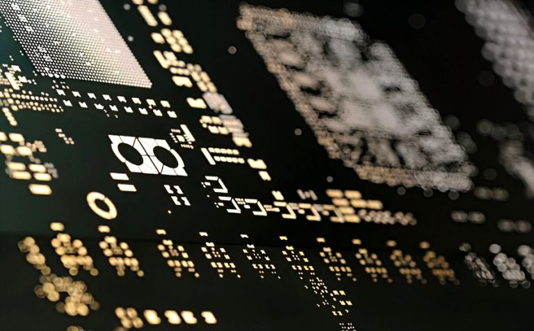
A PCB Stencil is a precision sheet used in surface mount technology (SMT) to deposit a controlled amount of solder paste onto designated PCB pads. It contains openings that correspond to the solder-pad locations on the printed circuit board, allowing solder paste to be transferred accurately during the Solder Paste Printing process.
PCB stencils are typically manufactured from stainless steel and may include fiducial-related features that support accurate alignment between the stencil and PCB. The stencil works together with a solder paste printer, squeegee, PCB support system, and inspection equipment to create a repeatable solder paste deposition process.
In modern PCB Assembly, solder paste printing is one of the most important processes because the amount and position of solder paste directly influence subsequent component placement and reflow soldering.
An appropriately designed stencil can help control solder volume, reduce solder bridging, improve component placement stability, and increase overall assembly consistency. This becomes especially important for fine-pitch components, miniature packages, BGA devices, QFN packages, and high-density PCB designs.

PCB Stencil Solder Paste Printing Process
The Stencil Printing process requires precise control of several variables, including stencil thickness, aperture geometry, solder paste properties, squeegee pressure, printing speed, separation speed, PCB support, and alignment accuracy.
The typical process includes the following steps.
1. Set Up the PCB and Stencil
The PCB is positioned on the solder paste printer using an appropriate support system. The PCB Stencil is securely mounted and aligned to prevent movement during printing.
Automatic printers generally use fiducial recognition or machine vision to align the PCB and stencil. Proper support beneath the PCB is also important, particularly for thin or flexible boards.
2. Prepare and Apply Solder Paste
An appropriate amount of solder paste is placed on the stencil surface in front of the squeegee.
Solder paste should be stored and handled according to the solder paste manufacturer’s specifications. Refrigerated storage is common for many formulations, but the exact storage temperature and allowable storage period vary by product.
Before printing, solder paste should be allowed to reach the recommended processing temperature and should be mixed or conditioned according to the manufacturer’s instructions.
3. Align the PCB and Stencil
The PCB and stencil are accurately aligned so that each stencil aperture corresponds to its intended PCB pad.
Alignment is particularly important for fine-pitch components because even a small offset can significantly affect solder paste deposition.
Modern printers can automatically compensate for small positional differences using fiducial recognition and machine-vision systems.
4. Print the Solder Paste
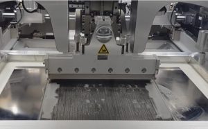
The squeegee travels across the stencil, forcing solder paste into the apertures.
During this operation, the squeegee angle, pressure, speed, paste rheology, stencil thickness, aperture geometry, and separation characteristics all influence printing quality.
After the squeegee passes over the stencil, solder paste remains on the corresponding PCB pads.
5. Separate the Stencil from the PCB
After printing, the stencil and PCB are separated in a controlled manner.
The separation process is particularly important for fine-pitch printing because uncontrolled separation can deform or disturb the deposited solder paste.
For advanced Stencil Printing, separation speed and release characteristics may be adjusted according to the PCB design and stencil geometry.
6. Inspect the Printed Solder Paste
After Solder Paste Printing, the deposited solder paste should be inspected to verify its position, volume, height, and coverage.
A solder paste inspection (SPI) system can measure parameters such as:
- Solder paste volume
- Paste height
- Deposit area
- X-Y position
- Shape and coverage
- Offset from the pad center
SPI provides quantitative feedback and can help identify printing-process drift before components are placed.
7. Clean the Stencil
Regular stencil cleaning is essential for maintaining consistent printing performance.
Solder paste residue can accumulate on aperture walls and the underside of the stencil. If the residue is not removed, it may cause insufficient paste transfer, bridging, print offset, or contamination of subsequent boards.
Depending on the production process, cleaning may be performed automatically using dry, wet, or vacuum-assisted methods.
Cleaning frequency should be determined by solder paste characteristics, aperture geometry, board design, and production conditions rather than applying one fixed interval to every product.
Key Considerations in PCB Stencil Design
Effective Stencil Design must account for the PCB layout, component package geometry, solder paste characteristics, manufacturing process, and required solder volume.
Stencil Geometry
Stencil thickness and aperture geometry are two of the most important design parameters.
Stencil thickness affects the amount of solder paste transferred through the apertures. A thicker stencil generally provides more solder paste, while a thinner stencil can be more suitable for fine-pitch components.
However, using a single thickness across an entire PCB can be challenging when the design contains both very small and relatively large components.
Aperture dimensions should therefore be optimized according to individual pad geometries and component requirements.
Area Ratio and Aspect Ratio
Two commonly discussed parameters in Stencil Design are the area ratio and aspect ratio.
The area ratio compares the aperture opening area with the aperture wall area. It is particularly relevant to fine-pitch stencil apertures because it influences solder paste release from the stencil.
The aspect ratio relates aperture width to stencil thickness.
Aperture dimensions should be evaluated according to the specific stencil manufacturing process, solder paste, component package, and required printing performance rather than applying one universal aperture reduction to every pad.
Aperture Reduction and Shape
Stencil apertures do not always have to be identical to the PCB pad dimensions.
A controlled aperture reduction or modification may be used to optimize solder volume and reduce the risk of bridging, solder balls, or excessive solder on specific component types.
Common aperture shapes include rectangular, square, rounded-rectangle, and other geometry optimized for particular component packages.
For example, QFN and fine-pitch components may require customized aperture segmentation or reductions to control solder volume and improve joint formation.
Stencil Materials
Stainless steel is the most widely used material for modern SMT stencils because it offers good mechanical strength, dimensional stability, corrosion resistance, and repeatability.
Other materials or specialized stencil constructions may be used for particular applications, but stainless steel is generally preferred for demanding production environments.
The quality of the aperture walls is also important. Smooth and accurately formed aperture walls can improve solder paste release and reduce paste retention.
Step Stencils
A step stencil, sometimes called a stepped stencil, contains areas with different local thicknesses.
This design is useful when one PCB contains both fine-pitch components that require a relatively thin stencil and larger components that require a greater solder paste volume.
For example, a thin region may support fine-pitch ICs while a thicker region can provide sufficient solder paste for larger components.
Step stencils require careful engineering because the transition areas must not interfere with printing or component placement.
PCB Stencil Manufacturing Technologies
Different Stencil Manufacturing technologies can be used to create stencil apertures. The manufacturing method influences aperture accuracy, wall quality, dimensional stability, and solder paste release.
Laser Cutting
Laser cutting is widely used for precision SMT stencil production.
A computer-controlled laser creates apertures directly in the stainless-steel sheet according to the approved stencil data.
The process can produce accurate and repeatable apertures and is well suited to fine-pitch and high-density PCB designs.
Laser-cut apertures can also be engineered with appropriate wall geometry to improve solder paste release.
Chemical Etching
Chemical etching uses a subtractive process to remove selected areas of metal and form the required stencil pattern.
The metal surface is prepared and coated with a suitable photoresist. The desired pattern is transferred to the surface, and an etchant removes the exposed material.
Although chemical etching can be used for certain stencil applications, aperture wall characteristics may differ from those produced by precision laser cutting.
Electroforming
Electroforming is an additive manufacturing process in which nickel is deposited to build the stencil structure around a patterned surface.
Electroformed stencils can provide very smooth aperture walls and may offer excellent paste-release characteristics for certain fine-pitch applications.
The appropriate manufacturing technology should be selected according to the required aperture dimensions, stencil thickness, production volume, and printing performance.
Common Solder Paste Printing Problems and Solutions
Poor stencil design, incorrect printing parameters, inadequate PCB support, or improper solder paste handling can result in printing defects.
| Problem | Possible Cause | Recommended Solution |
|---|---|---|
| Printing misalignment | Incorrect PCB-to-stencil alignment or movement during printing | Check fiducial alignment, PCB support, and printer calibration. |
| Solder bridging | Excessive solder paste, unsuitable aperture geometry, or printing offset | Optimize aperture dimensions, paste volume, alignment, and printing parameters. |
| Insufficient solder | Apertures too small, poor paste release, or blocked apertures | Review aperture design, stencil thickness, cleaning frequency, and paste condition. |
| Solder paste variation | Unstable printing parameters or paste condition | Control squeegee speed, pressure, paste handling, and stencil condition. |
| Solder balls | Excess solder paste, unsuitable paste behavior, or contamination | Review paste selection, aperture design, reflow profile, and stencil cleanliness. |
| Paste sticking to apertures | Poor release characteristics or contaminated stencil walls | Improve aperture geometry, stencil cleaning, and process control. |
| Paste smearing | Poor separation, insufficient PCB support, or excessive paste | Check support, separation parameters, stencil condition, and paste volume. |
The Role of SPI in SMT Assembly
SPI is an important process-control technology within modern SMT Assembly.
Unlike a basic visual inspection, SPI can measure the three-dimensional characteristics of solder paste deposits.
SPI data can be used to identify printing trends such as gradually decreasing solder volume, consistent positional offsets, blocked apertures, or abnormal paste height.
When SPI is integrated with the printing process, manufacturers can make adjustments before defective boards proceed to component placement and reflow.
This approach helps reduce downstream defects and improves process stability.
PCB Stencil and PCB Assembly Quality
The stencil has a direct relationship with the quality of PCB Assembly.
Solder paste printing determines the initial solder volume and location for many surface-mount solder joints. If the printed deposit is incorrect, later processes may not fully compensate for the problem.
For example:
- Excess solder may increase bridging risk.
- Insufficient solder may result in weak or open joints.
- Incorrect paste position can cause component misalignment.
- Uneven paste volume can affect solder joint consistency.
- Poor release can create recurring defects across multiple boards.
Therefore, stencil design should be considered during PCB design and DFM review rather than treated as a separate manufacturing activity.
PCB Stencil Maintenance
Proper stencil maintenance helps maintain stable printing quality.
Important practices include:
- Clean the stencil at an appropriate frequency.
- Inspect apertures for blocked or damaged openings.
- Check the stencil for warpage or mechanical damage.
- Store stencils in a controlled environment.
- Record stencil identification and usage history when required.
- Verify the stencil against the latest PCB revision.
- Avoid using damaged or contaminated stencils.
- Periodically verify critical aperture dimensions.
Stencil identification and revision control are particularly important for products that undergo frequent PCB design changes.
How to Optimize Stencil Printing
A reliable Stencil Printing process requires coordination between stencil design, solder paste, equipment, PCB support, and inspection.
Key optimization measures include:
- Select an appropriate stencil thickness.
- Optimize aperture geometry for each component type.
- Use suitable solder paste for the assembly process.
- Control solder paste storage and handling.
- Maintain consistent squeegee pressure and speed.
- Use appropriate PCB support.
- Control stencil separation.
- Perform regular stencil cleaning.
- Use SPI to monitor printing performance.
- Analyze printing defects using process data.
For high-density PCB designs, engineering review should focus not only on whether an aperture can be manufactured, but also on whether solder paste can be released consistently during production.
PCB Stencil for Single-Sided and Double-Sided PCB Assembly
PCB stencils can be used for both single-sided and double-sided PCB Assembly.
For single-sided assembly, the stencil primarily needs to accommodate the component side being populated.
For double-sided assembly, stencil design becomes more complex because components on both sides of the PCB may have different package sizes, solder requirements, and thermal characteristics.
Designers should also consider whether components placed on the first side may interfere with the printing, placement, or reflow process for the second side.
Choosing a PCB Stencil Manufacturer
When selecting a Stencil Manufacturing partner, important factors include:
- Stencil design capability
- Aperture manufacturing accuracy
- Material quality
- Laser or other manufacturing technology
- Ability to handle fine-pitch designs
- Step-stencil capability when required
- Inspection and dimensional verification
- Revision control
- Production consistency
- Technical communication
The lowest quoted price is not necessarily the most important consideration. Stencil quality can directly affect solder paste printing and therefore influence the overall SMT manufacturing process.
Kingda PCB Stencil and SMT Assembly Support
Kingda can support PCB manufacturing and SMT Assembly projects that require stencil-based solder paste printing.
Stencil requirements can be evaluated according to PCB layout, component package types, pad dimensions, solder paste characteristics, assembly process, and production requirements.
The manufacturing workflow can include stencil data preparation, aperture optimization, stencil fabrication, inspection, solder paste printing, SPI, component placement, reflow soldering, and subsequent inspection and testing.
For complex PCB designs, stencil requirements can also be considered during the DFM stage to identify potential printing risks before production begins.
Best Practices for PCB Stencil Applications
For consistent Solder Paste Printing, manufacturers should:
- Use the latest approved PCB design data.
- Match stencil design to the actual component and pad geometry.
- Select stencil thickness according to the complete PCB assembly.
- Optimize apertures for fine-pitch and large components.
- Maintain appropriate solder paste storage and handling conditions.
- Keep the stencil clean and inspect it regularly.
- Maintain accurate PCB support during printing.
- Control squeegee pressure, speed, and separation.
- Use SPI where process monitoring requires quantitative solder-paste data.
- Maintain stencil revision and production traceability.
Conclusion
A PCB Stencil is a critical tool in modern SMT manufacturing because it determines how solder paste is deposited onto PCB pads before component placement and reflow.
A successful Stencil Design requires careful consideration of stencil thickness, aperture geometry, area ratio, aspect ratio, component spacing, solder paste characteristics, and manufacturing tolerances. Laser cutting, chemical etching, and electroforming provide different approaches to Stencil Manufacturing, with the appropriate technology depending on the application’s precision and production requirements.
Consistent Stencil Printing also depends on solder paste handling, PCB support, printing parameters, stencil cleaning, and inspection. Combining a properly engineered stencil with SPI and controlled SMT Assembly processes can help reduce printing defects and improve overall PCB assembly reliability.
For projects requiring customized PCB production and assembly, Kingda can integrate stencil requirements with the broader PCB manufacturing and assembly process, helping ensure that stencil design and solder paste printing are considered as part of the complete manufacturing workflow.