




PCB Dimensions Guide: Standard Sizes, Thickness, Tolerances & IPC Standards
PCBs are the core carrier of modern electronic products – from smartphones and industrial control equipment to new energy vehicles, medical instruments, and AI servers, high‑quality PCBs are indispensable.
During PCB design, many engineers focus on circuit schematics, component placement, and signal integrity, but often overlook the importance of PCB dimensions. In fact, PCB dimensions are not just length and width; they also include board thickness, copper thickness, hole size, tolerances, edge clearance, and mechanical dimensions compliant with IPC standards. These parameters directly determine whether the PCB can be manufactured and assembled smoothly, and they affect product performance, reliability, and cost.
This article provides a comprehensive overview of PCB dimensions, including standard sizes, thickness specifications, tolerances, hole and via design, IPC standards, DFM recommendations, and cost references – helping engineers and procurement professionals quickly grasp the essentials.
1. What Are PCB Dimensions?
PCB dimensions refer to all mechanical parameters of a printed circuit board, including length, width, board thickness, copper thickness, hole sizes, via sizes, outline, edge clearance, and manufacturing tolerances. These dimensions affect electrical performance, signal integrity, EMI/EMC, thermal dissipation, mechanical strength, SMT assembly yield, and ultimately manufacturing cost.
2. Common Standard PCB Sizes
There is no single universal standard for PCB sizes; they vary by industry and application.
- Small PCBs: 20×20 mm, 50×50 mm, 100×100 mm – used in wearables, IoT modules, Bluetooth modules, consumer electronics.
- Medium PCBs: 150×100 mm, 200×150 mm – used in industrial control, power supplies, communication equipment, instrumentation.
- Large PCBs: 300×250 mm, 500×400 mm – used in industrial automation, telecom base stations, medical devices, network switches.
- Extra‑large PCBs: up to 1200×650 mm or even larger – used in AI server backplanes, data center equipment, aerospace, and military electronics.
3. PCB Thickness Standards
Board thickness significantly affects mechanical and electrical performance. The most common thickness is 1.6 mm (0.062 inch), which offers the lowest cost, mature processing, good mechanical strength, and best SMT compatibility – making it the default for most consumer and industrial electronics.
Other common thicknesses: 0.2, 0.4, 0.6, 0.8, 1.0, 1.2, 2.0, 2.4, and 3.2 mm. Ultra‑thin PCBs (0.1–0.4 mm) are used in flexible electronics, medical devices, smart cards, and camera modules. Thick boards (2.4–6.0 mm+) are used in high‑power supplies, solar inverters, energy storage, and motor drives.
4. Copper Thickness and Its Relation to PCB Dimensions
Copper thickness determines current‑carrying capacity and thermal performance. Standard options:
- 0.5 oz (~17 µm) – for high‑density, compact products
- 1 oz (~35 µm) – the industry standard for over 95% of PCBs
- 2 oz (~70 µm) – for LED lighting, industrial control, power PCBs, BMS
- Heavy copper (3–20 oz+) – for new energy vehicles, high‑current equipment, UPS, photovoltaic storage

5. PCB Dimensional Tolerances
Due to material shrinkage, drilling, lamination, etc., absolute zero tolerance is impossible. Typical tolerances:
- Outline tolerance: ±0.10 mm (standard), ±0.05 mm (high‑precision)
- Thickness tolerance: ±10% (e.g., 1.6 mm board allows 1.44–1.76 mm)
- Hole size tolerance: ±0.075 mm (mechanical), ±0.025 mm (laser)
- Copper thickness tolerance: ±10%
High‑reliability applications like automotive, medical, and high‑speed PCBs often require tighter controls.
6. PCB Hole and Via Design
Hole sizes affect soldering quality and interlayer reliability. Common through‑hole diameters: 0.20, 0.30, 0.40, 0.50, 0.80, 1.00 mm. Standard vias: drill 0.20–0.30 mm, pad 0.45–0.60 mm. Microvias (0.075–0.15 mm) are used in HDI PCBs, smartphone motherboards, AI servers, and high‑speed communication boards.
7. Edge Clearance Requirements
Edge clearance is the minimum distance from traces, copper, or pads to the board edge. Recommended minimum is 0.25 mm, with 0.5 mm preferred. For high‑voltage designs, clearance may need to be 2 mm, 4 mm, or more to meet insulation and safety requirements. Proper clearance prevents electrical breakdown, delamination, edge cracking, and SMT defects.
8. IPC Standards for PCB Dimensions
Key IPC standards governing PCB dimensions and quality include:
- IPC‑A‑600 – Acceptance of printed boards
- IPC‑2221 – Generic standard on printed board design
- IPC‑6012 – Qualification and performance specification for rigid PCBs
- IPC‑6013 – For flexible PCBs
- IPC‑6018 – For high‑frequency PCBs
Following IPC standards ensures quality consistency and meets global OEM procurement requirements.
9. How PCB Dimensions Affect Manufacturing Cost
Larger PCBs consume more material, require more drilling, and take longer processing time – increasing cost. Thicker boards need more prepreg and lamination cycles, also raising cost. Tighter tolerances increase inspection effort and reduce yield, driving up price. HDI and micro‑via designs involve laser drilling and sequential lamination, making them much more expensive than standard boards.
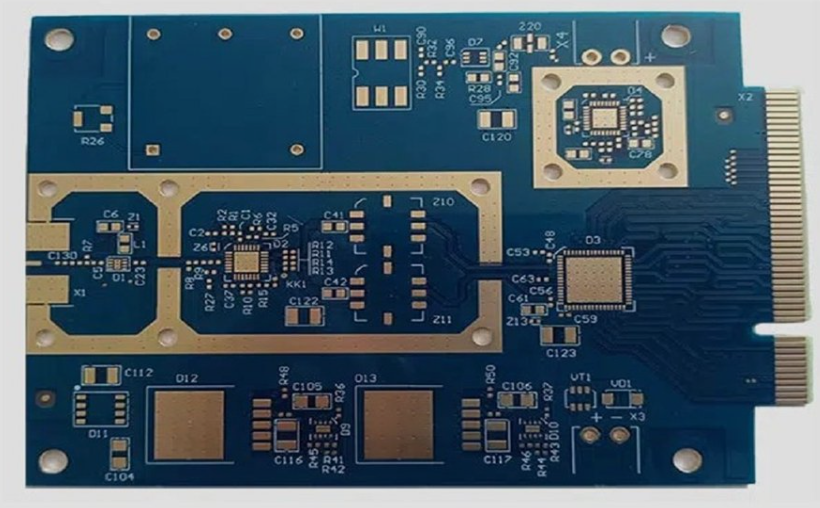
10. DFM Recommendations for PCB Dimensions
To improve manufacturability (DFM), we recommend:
- Use standard board thicknesses (e.g., 0.8, 1.0, 1.6 mm)
- Avoid overly tight tolerances on non‑critical dimensions
- Plan board size to maximize panel utilization
- Strictly follow IPC design guidelines
- Ensure adequate edge clearance
- Conduct a DFM review with your PCB manufacturer early in the project
For professional design support, visit our PCB design & layout service.
11. gopcb’s PCB Manufacturing Capabilities
As a professional PCB and PCBA one‑stop service provider, gopcb is committed to delivering high‑quality PCB solutions to electronics manufacturers worldwide.
- Layer count: 1–80 layers
- Max board size: 1200 mm × 650 mm
- Min thickness: 0.1 mm; max thickness: 10 mm
- Min mechanical drill: 0.15 mm; min laser microvia: 0.075 mm
- Copper weight: 0.5–20 oz
- Supports impedance control, high‑speed, HDI, heavy copper, rigid‑flex, and high‑layer boards
- Integrated services: PCB fabrication, SMT assembly, component procurement, and turnkey assembly
gopcb is certified under ISO 9001, UL, RoHS, and meets IPC Class 2/Class 3 standards. Explore our PCB manufacturing and SMT PCB assembly capabilities, as well as our turnkey assembly solutions.
12. PCB Manufacturing Price Reference (2026)
Prices vary with dimensions, layer count, material, copper weight, surface finish, process complexity, and order volume.
- Prototype (2‑layer FR4, 100×100 mm, 5–10 pcs): about $5–30
- Low volume (100–500 pcs, 4‑layer): about $0.8–8 per board
- High volume (10,000+ pcs, 4‑8 layers): about $0.10–3 per board
- HDI PCBs: about $20–300 per board depending on layers, microvia count, and complexity
For an accurate quote, provide Gerber files and a BOM for a DFM analysis.
13. Frequently Asked Questions
Q1: What is the most common PCB thickness?
1.6 mm (0.062 inch) is the most widely used standard thickness due to its balance of strength, cost, and assembly compatibility.
Q2: What is the maximum PCB size available?
Typical manufacturers support up to 500×500 mm; gopcb can produce up to 1200×650 mm for large‑format boards.
Q3: Does PCB thickness affect high‑speed signal transmission?
Yes. Thickness influences dielectric thickness, impedance control, and signal integrity. High‑speed designs must consider thickness, Dk, and stack‑up.
Q4: What are typical PCB dimensional tolerances?
Outline tolerance is typically ±0.10 mm, with ±0.05 mm for high‑precision; thickness tolerance is ±10%.
Q5: Why is PCB dimension design important?
Proper dimensions ensure fit, assembly, electrical performance, thermal management, yield, and cost – making it a critical aspect of PCB design.
14. Conclusion
PCB dimensions encompass more than just length and width – they include thickness, copper weight, hole sizes, tolerances, edge clearance, and IPC specifications. Scientifically designed dimensions improve product reliability, optimize manufacturing, and reduce overall cost.
For high‑end applications like high‑speed communications, automotive, medical, AI servers, new energy, and industrial control, it is essential to consider dimension standards and DFM early, and to collaborate with an experienced PCB manufacturer. gopcb offers advanced equipment, strict IPC quality control, and rich experience in high‑layer, HDI, and heavy‑copper PCBs – providing reliable, high‑quality PCB fabrication and PCBA services to help you bring your products to market efficiently.
Get started with our prototype PCB assembly or low‑volume assembly services, and let us support your project from design to production.


