



PCB Gold Plating Types: ENIG, Hard Gold and Thickness
Gold appears on a printed circuit board for two reasons, and they rarely coexist. One is chemistry: a thin, dense gold layer over nickel keeps copper from oxidising and preserves a solderable or wire bondable surface for months. The other is mechanics: a thick, hardened gold layer resists the wear of repeated insertion, which is why edge connectors and test pads are plated differently from the rest of the board.
Confusing the two is the most common mistake in specifying a finish. A hard gold on a solder pad causes brittle joints, and a thin immersion gold on a connector that is mated a thousand times wears through in the field. This article explains how the common gold finishes differ and how to specify the one the application actually needs.
Why a Nickel Barrier Comes First
Gold does not plate directly onto copper in a reliable way for most finishes. Copper diffuses into gold even at room temperature, so a thin gold layer over bare copper becomes a gold and copper alloy within weeks and loses both its solderability and its low contact resistance.
The nickel layer between them acts as a diffusion barrier, typically 3 to 6 micrometres thick. Its quality decides the performance of the finish: a porous or poorly adhered nickel layer allows the underlying copper to migrate to the surface, and the resulting failure appears as a solder joint that will not wet or a contact resistance that drifts upward over time.

Immersion Gold and Electroless Nickel
An electroless nickel and immersion gold finish deposits the nickel by chemical reduction and the gold by a displacement reaction that stops once the nickel is covered. The result is a very thin gold layer, usually around 0.05 to 0.1 micrometre, over a uniform nickel barrier.
That thickness is enough for solderability and for aluminium wire bonding, and it is the reason the finish is popular on dense boards: it is flat, it does not require a connection to every pad, and it works on fine pitch components. It is not, however, intended for repeated mechanical contact, because there is almost no gold to wear away.
Hard Gold for Wear and Mating Cycles
Hard gold, or gold over nickel applied by electroplating, is alloyed with a small amount of cobalt or nickel and deposits to a much greater thickness, commonly 0.5 to 1.5 micrometres and sometimes more. The alloy gives it a hardness that resists abrasion, which is what a card edge, a spring contact or a pogo pad needs.
Because electroplating requires a current path, every pad to be plated must be connected, and the plating buss has to be removed afterwards. That added processing is why hard gold is normally applied selectively to the connector area rather than to the whole board, and why the fabrication drawing has to state which pads are in scope.
Choosing Between Them and Specifying Thickness
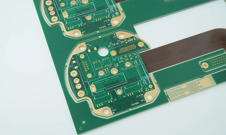
The decision follows the function. Pads that will be soldered need a thin, flat, solderable finish. Surfaces that will be touched, inserted or probed repeatedly need a thick, hard layer. Where a board has both, the finish is usually split, with immersion gold over the component area and hard gold on the edge fingers.
Thickness is specified in micrometres, and it should be stated with the measurement method and the acceptance test. A drawing that says simply gold is not a specification. Where the pads also serve as test points, consider the probe pressure and the number of touches the product will see, because a probe marks the surface whether the plating was specified for it or not.
Other Finishes and Where Gold Is Not Required
Gold is not the only way to protect a copper surface. Hot air solder levelling produces a thick, solderable coating that survives multiple reflow cycles and is inexpensive, at the cost of a surface that is not flat enough for the finest pitch components. Immersion tin and immersion silver provide a flat, solderable surface with a limited shelf life, and an organic solderability preservative gives the flattest and cheapest option of all, provided the board is assembled soon after fabrication and handled with care.
Where a gold plating process is used, it is usually because the application needs either a very long shelf life, a wire bondable surface or a low and stable contact resistance. Where none of those apply, a simpler finish will usually serve the product better, because every additional metal layer adds a process step, a waste treatment requirement and a failure mode. The decision should therefore begin with a question about the surface function rather than with a preference for gold.
Process Control and Common Defects
The defects that matter in a gold finish are rarely about the gold itself. Black pad, a condition in which the nickel surface beneath the immersion gold is attacked during the displacement reaction, produces a solder joint that wets poorly and fails at low load, and it is the reason the nickel bath chemistry and the gold thickness are controlled so closely. Gold thickness that is too great for the application slows the dissolution of gold into the solder and produces brittle intermetallic layers, which is why the specification should set an upper limit as well as a lower one.
Hard gold has its own failure modes. Plating that is too thin wears through at the corners of a card edge finger, where the contact pressure is highest, and plating with excessive stress cracks along the finger during insertion. Both are controlled by the current density, the bath composition and the thickness measurement, and both are visible in a wear test that mates the connector to the specified cycle count and then examines the contact area rather than the whole finger.
Related reading: PCB manufacturing processes, PCB manufacturing tolerances, lead free versus leaded solder, and PCB design quality characteristics.
The choice also interacts with the assembly process. A board finished with immersion gold can be stored for many months before assembly, while an organic preservative demands a short interval between fabrication and reflow, and a product built in small batches from stock may not be able to honour that interval. Where the assembly includes aluminium wire bonding, the gold thickness and the nickel surface roughness both have to satisfy the bonding specification, because a bond that lifts after encapsulation leaves no opportunity for rework.
FAQ
Why does gold sometimes look dull or discoloured? Usually because of contamination or oxidation of the nickel layer, or because the gold was deposited over a surface that had already begun to corrode. The appearance is a symptom of the barrier layer, not of the gold itself.
Can hard gold be soldered? It can, but the joints are brittle and the thicker gold dissolves slowly into the solder, which is why hard gold is best kept away from solder joints and used only for contact surfaces.
How thick should a gold finish be? Around 0.05 to 0.1 micrometre for immersion gold used for soldering, and 0.5 to 1.5 micrometres for hard gold used on mating surfaces. The number follows the wear or the bonding requirement, not the price.



1 Comment
Gold Finger Bevel Angle and Edge Design
[…] reading: PCB gold plating types, board outline and mounting design, PCB manufacturing tolerances, and press fit connector […]