PCB Industry Trends: 10 Technologies Shaping the Future of PCB Manufacturing
The PCB industry is entering a new stage of technological transformation. Rapid growth in AI computing, automotive electronics, 5G communications, IoT, robotics, and other advanced applications is driving innovation across PCB materials, circuit design, manufacturing processes, and production models.
Traditional PCB manufacturing is evolving toward higher density, higher frequency, greater reliability, intelligent production, and more sustainable processes. At the same time, emerging applications are creating new requirements for PCB performance and integration.
This article explores 10 major PCB industry trends shaping the market in 2025 and explains how these technologies may influence PCB design, manufacturing, and assembly.
1. High-Frequency and High-Speed Materials Are Becoming Critical
The rapid expansion of AI servers, high-speed networking, data centers, and advanced communication equipment is increasing demand for high-frequency and high-speed PCB materials.
At higher data rates, conventional materials may introduce excessive dielectric loss, conductor loss, and signal distortion. As a result, PCB designers and manufacturers are increasingly evaluating materials with lower dielectric loss, controlled dielectric properties, and improved thermal stability.
Materials and material technologies used in demanding applications may include:
- Low-loss resin systems
- PTFE-based materials
- High-performance hydrocarbon/ceramic materials
- Low-Dk and low-Df laminates
- Low-profile copper foil
- Very-low-profile copper for high-speed signal applications
- Advanced glass fabrics with controlled electrical characteristics
Copper surface roughness is also becoming increasingly important because conductor loss can become a significant factor at high frequencies.
However, material selection should not be based solely on a material’s advertised Dk or Df. Stack-up design, copper roughness, trace geometry, impedance requirements, operating frequency, temperature, and manufacturing tolerances all need to be considered.
For demanding high-speed designs, accurate PCB Design Layout and fabrication process control are essential.
2. High-Layer-Count and High-Density PCB Manufacturing Continues to Advance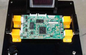
As electronic systems become more powerful and compact, PCB designs are moving toward higher layer counts and greater routing density.
AI computing hardware, networking equipment, advanced industrial electronics, and other high-performance systems may require complex multilayer structures to provide sufficient power distribution, signal routing, and electromagnetic control.
Key technologies include:
- High-layer-count multilayer PCBs
- HDI structures
- Microvias
- Blind and buried vias
- Sequential lamination
- mSAP and SAP processes
- Fine-line and fine-space routing
- Advanced laser drilling
High-density manufacturing allows designers to route more signals within a limited board area. However, increasing density also raises manufacturing challenges involving registration, lamination, via reliability, plating, impedance control, and yield.
For this reason, successful high-density PCB production requires close cooperation between PCB designers and manufacturers before fabrication begins.
3. Embedded Components Are Driving Greater System Integration
Embedded component technology is expanding the functional capabilities of PCBs by integrating selected components into the board structure rather than placing everything on the external surface.
Depending on the application and manufacturing process, embedded technologies can be used for certain passive components, semiconductor devices, power components, or other specialized structures.
Potential advantages include:
- Reduced overall system size
- Shorter electrical interconnections
- Improved electrical performance
- Better space utilization
- Potential thermal-management benefits
- Greater system integration
However, embedded components also create significant manufacturing challenges. Precise placement, lamination, thermal management, inspection, repairability, and long-term reliability must all be addressed.
Therefore, embedded PCB technology is most suitable for applications where its integration benefits justify the additional manufacturing complexity.
4. Advanced Package Substrates Are Evolving Rapidly
Advanced package substrates sit between semiconductor devices and conventional PCBs, providing increasingly dense electrical interconnections for high-performance chips.
The growth of AI processors, high-performance computing, networking ASICs, and advanced semiconductor packages is increasing demand for technologies such as:
- FC-BGA substrates
- Fine-line substrate technologies
- Advanced interconnect structures
- Glass-core substrate research
- Chiplet-related packaging technologies
- Co-packaged optics and other advanced packaging architectures
These technologies require extremely precise manufacturing because package-level interconnects are significantly smaller and more sensitive to dimensional variation than many conventional PCB structures.
Flatness, warpage, line width, registration, dielectric performance, and via reliability become especially important as interconnect density increases.
It is important to distinguish advanced package substrates from conventional PCBs: although they share some manufacturing principles, their design rules, materials, process requirements, and inspection requirements can be substantially different.
5. Intelligent Manufacturing Is Transforming PCB Production
Automation and digitalization are becoming increasingly important in modern PCB Manufacturing Technology.
Instead of relying heavily on manual operation, manufacturers are adopting automated equipment, process monitoring, digital production management, and machine-assisted inspection.
Important technologies include:
Laser Direct Imaging
LDI technology enables highly accurate imaging of circuit patterns and is particularly useful for fine-line and high-density PCB manufacturing.
Automated Lamination and Material Handling
Automated systems can improve consistency in multilayer production while reducing manual handling and process variation.
Automated Optical Inspection
AOI systems help identify defects such as missing features, open circuits, short circuits, insufficient copper patterns, and other visual abnormalities.
X-Ray Inspection
X-ray inspection is particularly valuable for examining internal structures and selected assembly-related features that cannot be evaluated through conventional visual inspection.
The long-term trend is toward greater integration between manufacturing equipment, inspection systems, production data, and process-control software.
6. Automotive PCBs Are Moving Toward Higher Reliability and Greater Diversity
The rapid development of electric vehicles, advanced driver-assistance systems, connected vehicles, and intelligent cockpits is expanding the range of PCB technologies used in automotive electronics.
Different automotive systems require different PCB characteristics.
For example:
- Power electronics may require high-current or heavy-copper structures.
- ADAS and radar systems can require high-frequency materials and controlled impedance.
- Infotainment systems may use high-density multilayer and flexible technologies.
- Battery-management systems require reliable electrical and thermal performance.
- Vehicle control systems require stable operation under demanding environmental conditions.
Automotive PCB manufacturing therefore places strong emphasis on process consistency, traceability, reliability, and application-specific qualification.
Not every automotive PCB requires the same material or certification framework. Requirements should be determined according to the vehicle system, electrical conditions, operating environment, and customer specifications.
7. Additive and 3D Printing Technologies Are Opening New Possibilities
Additive manufacturing and 3D printing are attracting increasing attention in specialized electronics applications.
Unlike conventional subtractive PCB manufacturing, additive approaches build structures layer by layer. This can create opportunities for unusual geometries, customized structures, rapid development, and certain specialized electronic components.
Potential applications include:
- Customized electronic structures
- Ceramic electronic components
- Miniaturized electronics
- Rapid prototyping
- Specialized RF structures
- Aerospace and advanced industrial electronics
However, 3D-printed electronics should not be viewed as a universal replacement for conventional PCB manufacturing.
For high-volume standard PCBs, conventional processes remain highly competitive. Additive technologies are more promising where design flexibility, customization, complex geometry, or specialized materials provide a clear advantage.
8. Green PCB Manufacturing Is Becoming a Competitive Advantage
Environmental requirements are becoming an increasingly important part of the global electronics supply chain.
PCB manufacturing involves chemical processes, water consumption, energy use, wastewater treatment, and material management. As environmental regulations and customer sustainability requirements become stricter, manufacturers are under increasing pressure to improve resource efficiency.
Green manufacturing initiatives may include:
- Reducing water consumption
- Improving wastewater treatment
- Reducing chemical consumption
- Improving energy efficiency
- Optimizing material utilization
- Reducing production waste
- Selecting environmentally preferable materials where appropriate
- Improving recycling and resource recovery
- Monitoring carbon emissions
Environmental compliance is increasingly becoming more than a regulatory requirement. For international customers, responsible manufacturing practices can also become an important factor when evaluating long-term suppliers.
9. One-Stop PCB Services Are Reshaping the Business Model
Electronics development cycles are becoming shorter, while engineering teams increasingly expect suppliers to provide support beyond bare-board fabrication.
This is driving demand for integrated PCB services covering multiple stages of product development.
A modern supplier may support:
- PCB design review
- DFM analysis
- PCB prototyping
- PCB fabrication
- Component sourcing
- SMT assembly
- Through-hole assembly
- Mixed-technology assembly
- Functional testing
- Low-volume or mass production
For customers, integrating these processes can reduce supplier coordination and shorten the time between design completion and working prototypes.
For example, companies developing a new electronic product may begin with a prototype PCB, validate the design, and then transition to low-volume production before moving toward larger-scale manufacturing.
For customers requiring broader supply-chain support, turnkey production can combine PCB fabrication, component procurement, and assembly into a more streamlined workflow.
Turnkey PCB Assembly
10. Satellites, Robotics, and Other Emerging Applications Are Creating New PCB Requirements
Emerging industries are creating specialized requirements that differ significantly from traditional consumer electronics.
Low-Earth-Orbit Satellites
Space electronics may need to operate under demanding conditions involving temperature extremes, vibration, vacuum, radiation exposure, and strict weight constraints.
PCB material selection and reliability requirements therefore need to be determined according to the specific mission and equipment environment.
Humanoid and Industrial Robots
Robotics systems combine sensors, processors, motor controllers, communication modules, power electronics, and compact mechanical structures.
This creates demand for:
- High-density multilayer PCBs
- Flexible PCBs
- Rigid-flex PCBs
- High-speed signal interconnects
- High-current power boards
- Miniaturized control boards
Flexible circuits can be particularly useful in moving joints or locations where conventional rigid boards cannot provide sufficient mechanical flexibility.
A Quick Comparison of the 10 PCB Technology Trends
| Trend | Main Driver | Key PCB Requirement |
|---|---|---|
| High-frequency materials | AI, networking, 5G | Low loss and controlled electrical properties |
| High-density manufacturing | AI and compact electronics | Fine lines, microvias, multilayer integration |
| Embedded components | Miniaturization | High integration and precise manufacturing |
| Advanced substrates | Semiconductor packaging | Ultra-fine interconnects and dimensional control |
| Intelligent manufacturing | Automation and quality | Process monitoring and automated inspection |
| Automotive electronics | EVs and ADAS | Reliability and application-specific performance |
| 3D/additive manufacturing | Miniaturization and customization | Complex structures and design flexibility |
| Green manufacturing | Environmental requirements | Resource efficiency and process control |
| One-stop services | Faster product development | Integrated fabrication and assembly |
| Satellites and robotics | Emerging applications | Specialized materials and high reliability |
What These Trends Mean for PCB Buyers
For electronics companies sourcing PCBs internationally, these technology trends have several practical implications.
1. Evaluate More Than Price
A low unit price does not necessarily represent the lowest overall cost. Yield, reliability, engineering support, lead time, and rework risk can have a major impact on total project cost.
2. Match Materials to the Application
High-speed, RF, power, automotive, aerospace, and general-purpose electronics may require completely different PCB materials.
Material selection should consider electrical performance, thermal requirements, mechanical properties, operating temperature, reliability, and cost.
3. Consider Manufacturability Early
A PCB design that works electrically may still create manufacturing problems.
Design teams should review:
- Trace width and spacing
- Via structures
- Layer stack-up
- Impedance requirements
- Copper distribution
- Thermal management
- Component clearances
- Manufacturing tolerances
A DFM review before production can identify potential problems before they become expensive manufacturing issues.
4. Choose a Supplier With the Right Process Capability
Not every PCB manufacturer is equipped for high-layer-count, HDI, high-frequency, heavy-copper, flexible, or other specialized PCB technologies.
Before placing an order, confirm that the supplier’s actual manufacturing capabilities match the technical requirements of the project.
For more information about fabrication capabilities and production considerations, see Gopcba’s:
How Gopcba Supports Evolving PCB Requirements
As PCB technology becomes more specialized, manufacturers need to provide more than basic fabrication.
Gopcba supports customers throughout different stages of PCB development, including prototype development, PCB manufacturing, component procurement, and assembly.
For projects that require flexible order quantities and rapid product validation, Low-Volume PCB Assembly can help engineering teams move from prototype testing to early production more efficiently.
The right manufacturing strategy ultimately depends on the product’s technical requirements, production volume, reliability targets, and expected lifecycle.
Conclusion
The PCB Industry Trends emerging in 2025 reflect a broader transformation across the electronics industry.
AI computing and high-speed networking are accelerating demand for low-loss materials and high-density interconnects. Automotive electronics are increasing requirements for reliability and specialized PCB technologies. At the same time, intelligent manufacturing, environmental sustainability, integrated supply-chain services, and emerging applications such as robotics and satellites are changing how PCBs are designed and produced.
The future of Advanced PCB Manufacturing will not be defined by a single technology. Instead, competitive PCB solutions will increasingly depend on the combination of advanced materials, precise manufacturing processes, intelligent quality control, effective design-for-manufacturing practices, and responsive supply-chain support.
For PCB buyers and engineering teams, understanding these trends can help them select appropriate technologies, evaluate suppliers more effectively, and build a more reliable path from PCB prototype to production.