Plasma Treatment in PCB Fabrication: Desmear and Surface Activation
Plasma treatment has moved from a specialty step to a routine one in PCB fabrication, because the surfaces that modern boards rely on, including polyimide, PTFE, filled resins and laser-drilled via walls, are chemically inert and do not wet reliably without preparation. Plasma surface activation uses a partially ionised gas to clean, etch and chemically modify those surfaces, raising surface energy so the next process can bond to them. The same chamber serves desmear, carbon removal after laser drilling and adhesion promotion before lamination, which makes it one of the most versatile tools on the shop floor.
What plasma actually does to a board surface
Inside a vacuum chamber, an RF field ionises a process gas into ions, electrons and radicals. Those species travel at high velocity, and their combined physical bombardment and chemical reaction removes organic contamination without leaving solvent residue behind. Oils from handling, mold release agents and photoresist residue are converted into volatile compounds and pumped away. On polymers the bombardment also breaks bonds in the top molecular layers and introduces polar groups, which is exactly what raises surface energy and lets aqueous chemistry wet the surface evenly. Because the reaction is confined to a few nanometres, the bulk properties of the laminate are unchanged. No solvent is consumed, so the process is also easier to permit than a wet line.
Batch, in-line and localized treatment
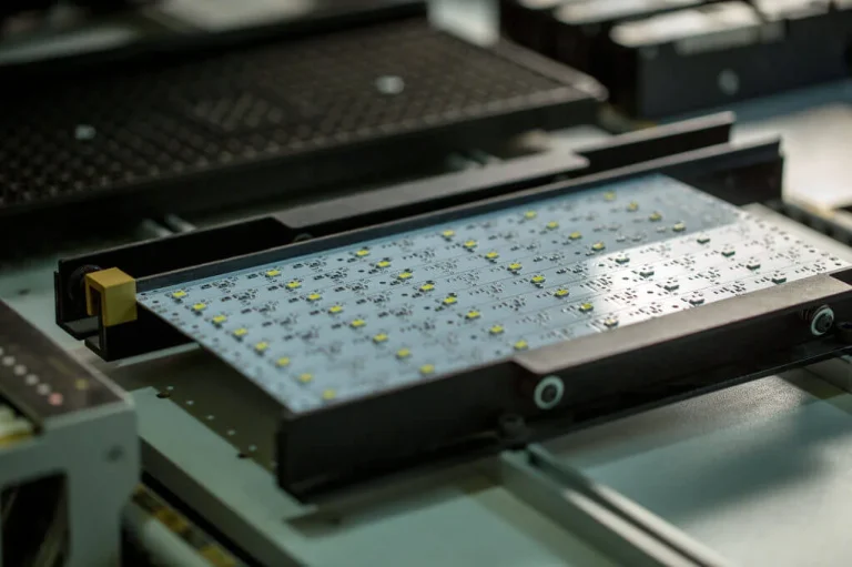
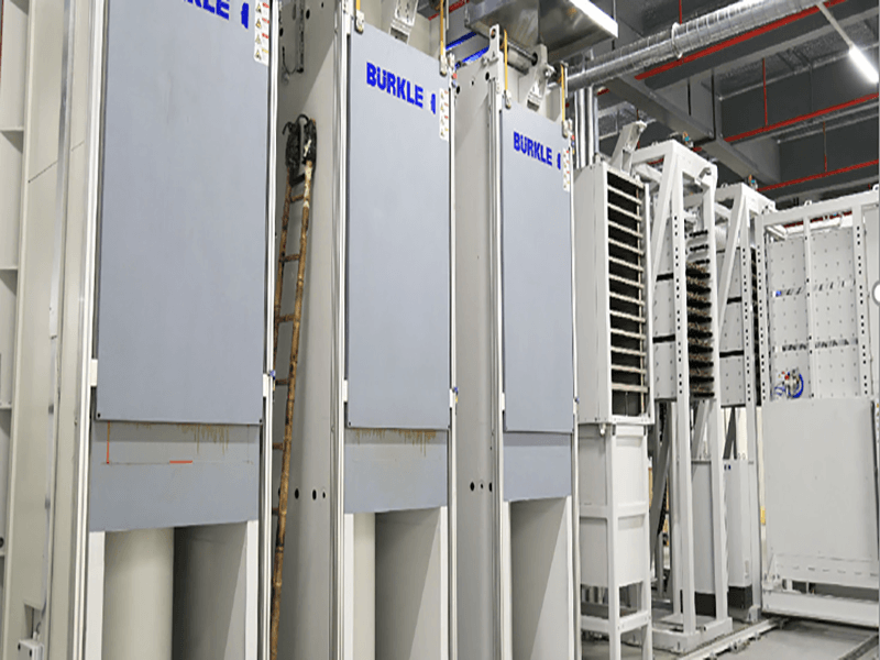
Plasma systems come in batch chambers, in-line tunnels and localized heads. A batch chamber treats many panels at once and gives the most uniform result, which suits desmear across a full panel of small holes. An in-line tunnel runs panels continuously, so the treatment keeps pace with a high-volume line instead of becoming a bottleneck. A localized head mounted on a robot arm can be positioned over a specific area, which allows activation of a fine outline or a single connector footprint without exposing the rest of the assembly. Processes run at very high speed in all three configurations, because the active species reach the surface as soon as the gas is energized rather than diffusing through a liquid boundary layer.
Desmear on multilayer and rigid-flex boards
Drilling and laser ablation leave resin smear on the copper barrel walls, and if that smear is not removed the plated copper cannot make reliable contact with the inner-layer pads. Plasma desmear removes the residue thoroughly and improves hole wall adhesion, which protects against open circuits that only appear after inner-layer plating. Rigid-flex, multilayer flex and adhesive-based builds are the most demanding cases, because their acrylic and epoxy adhesive systems smear more readily than rigid FR-4. High-aspect-ratio microvias in thick laminate benefit as well: wet chemical desmear struggles to exchange chemistry deep inside a narrow hole, while the plasma species reach the full barrel.
High-frequency laminates before copper deposition
PTFE and other low-loss laminates are among the most chemically inert materials in a PCB shop, and electroless copper will not anchor to them without pretreatment. Plasma surface activation modifies the hole wall before deposition, giving the catalyst a polar, wettable surface. That step is what suppresses the black hole and void defects that otherwise show up as blowholes and unreliable interconnects after thermal cycling. Because the treatment is physical as well as chemical, it reaches the full depth of the hole regardless of the drilling method, which is an advantage on thick high-frequency backplanes where wet activation chemistry is prone to incomplete exchange.
Solder mask and legend adhesion
Weak solder mask adhesion is a quiet failure mode. The board passes electrical test, then the mask lifts along a trace after reflow or thermal cycling and exposes copper to the environment. Activating the board surface before mask coating and legend printing gives the resist a higher-energy surface to bond to, which reduces flaking and peeling on fine-pitch features. The same benefit applies before conformal coating, where uniform wetting of the surface determines how well the coating seals around components and edges.
Laser-drilled vias and carbon removal
Laser drilling of blind vias leaves carbonised resin on the via wall, and that carbon layer is both conductive enough to cause leakage and inert enough to block plating adhesion. Plasma cleaning removes the residue without regard to via diameter, and the effect is most pronounced in microvias below about 50 microns, where mechanical and chemical cleaning cannot reach reliably. Treating vias at this stage protects the plating step that follows.
Dry film residue and fine-line etching
Fine-line pattern plating leaves dry film residue behind after development, particularly where the film was compressed into narrow spaces. If that residue survives into the etch step it shields copper that should have been removed, and the result is a short between adjacent traces. A plasma step after development removes the trapped film before etching. The same clean, activated surface also improves resist adhesion on the next layer, so the benefit compounds across a sequential-lamination build.
Polyimide roughening before lamination and stiffeners
Flexible circuits expose the most demanding adhesion problem of all. Polyimide is smooth and inert, and both coverlay lamination and stiffener bonding depend on a mechanical and chemical key at the interface. Plasma roughening before lamination can raise the peel strength by roughly an order of magnitude compared with an untreated surface, which is the difference between a flex that survives repeated bending and one that delaminates in the field. The same surface preparation before final packaging and before gold wire bonding raises wire pull strength and improves long-term connection reliability. Review it alongside the plating chemistry so that surface preparation and deposition are specified as one process window rather than two.
Two scheduling notes follow from all of this. Activated surfaces do not stay activated: the polar groups reorient and contamination returns within hours, so plasma treatment must sit immediately before the next wet process rather than at the end of a shift. And the treatment window should be defined by a measurable result, such as a water contact angle or a peel test, not by a fixed recipe carried over from another product. Conformal coating and board protection and the rules collected in manufacturable PCB design guidelines both assume a clean, high-energy surface; gopcb specifies the plasma step as part of that chain.
Why plasma suits fine features
Mechanical scrubbing and pumice cleaning work on flat, open surfaces, but they cannot reach inside a 50 micron via or under a fine-pitch component. Plasma reaches every exposed surface in the chamber, including the walls of deep holes and the gaps between closely spaced traces, and it does so without abrasion that could shift or damage fine features. That reach is the reason the process is specified on high-density builds rather than reserved for contamination emergencies. It also avoids the rinse and drying steps that follow a wet clean, which removes a source of water spots and trapped moisture in a laminated stack.
FAQ
Does plasma treatment replace chemical desmear entirely? Not always. Plasma handles the resin smear and carbonised residue very effectively, but some builds still use a permanganate or other wet desmear step for bulk removal. The two are complementary, and the sequence depends on the laminate and the aspect ratio.
How long does an activated surface stay active? Hours, not days. Surface energy decays as the treated surface adsorbs moisture and airborne organics, so the next process should follow within the same shift. If a panel must wait, re-treat it rather than assume the activation survived.
Can plasma damage the laminate? The reaction depth is limited to the top few nanometres under a controlled recipe, so the bulk material is safe. Damage occurs when dwell time or power is pushed far beyond the validated window, which is why the process should be locked to a measured result.