Server PCB: Architecture, Materials and Manufacturing Requirements
A server PCB is a large, high-layer-count board that must deliver enormous current to a processor and move data at rates that leave very little margin in the channel. It is fabricated in small volumes compared with consumer products, and the tolerance for failure is correspondingly small.
Designing one means balancing power delivery, signal integrity, thermal management and mechanical stiffness on a board that may be half a metre across.
Architecture and Layout
The board is organized around the processor sockets, the memory channels and the expansion slots. Memory traces dominate the routing, because each channel requires matched, impedance-controlled lines between the processor and the module connectors.
Connector and socket placement is fixed by mechanical standards, so the layout is constrained from the beginning. The remaining freedom is in the routing layers and the power distribution, and those two compete for the same stack.
<img src="https://www.gopcba.com/wp-content/uploads/2026/08/pcb7.jpg" alt="Server PCB with high layer count and back drilled vias” />
Layer Count and Stackup
Server boards commonly run from sixteen to thirty layers or more, with a significant fraction dedicated to ground and power planes. The plane pairs provide the low-impedance power distribution and the reference planes that the high-speed buses require.
Stackup design is a compromise between signal layer count, plane pairs and total thickness. Thickness affects drilling and aspect ratio, and it also affects mechanical stiffness, which matters on a large board.
Power Delivery
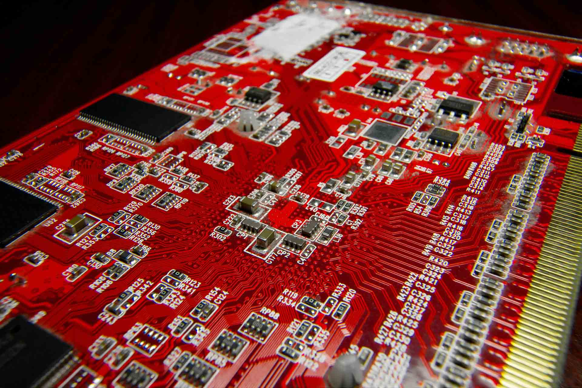
Power delivery is the dominant design problem. A processor may draw hundreds of amps at a low voltage, and the delivery network must hold the voltage within a narrow window across a wide frequency range.
Multiple plane pairs, dense via arrays under the socket and a mixture of bulk and ceramic capacitors work together. Inductance in the vertical path is usually the limiting factor, which is why the number of vias per connection is high and their placement is planned rather than incidental.
Voltage regulator placement also matters. The modules should be close to the load, and their output current should flow to the socket without passing through shared conductors that carry other currents.
High-Speed Buses
Memory, storage and interconnect buses each have their own requirements. Differential pairs need continuous reference planes, matched lengths and controlled impedance, and single-ended buses need a defined return path and controlled loading.
Insertion loss and crosstalk budgets are allocated across the board, the connector and the package. Where the total is tight, low-loss material is used on the signal layers that carry the fastest interfaces, and back drilling removes via stubs.
Reference plane continuity is verified across the entire channel. A plane split under a fast bus is the most common cause of a channel that fails its eye diagram despite correct routing.
Back Drilling and Via Design
On a thick board, a plated through-hole that connects to an inner layer leaves a stub below the connection. That stub resonates and distorts the signal, so back drilling removes it to a controlled depth.
Back drilling adds cost and requires tight depth control, so it is applied selectively to the nets that need it rather than to every via. The design drawing must identify which vias require it and to what depth.
Connectors and Mechanical Design
Server boards use press-fit connectors for power and for the backplane interface. Press-fit requires a controlled hole diameter and plating thickness, and the board thickness tolerance becomes a functional dimension.
Mechanically, a large board must stay flat enough to insert into a chassis and to accept large socketed components. Copper balance, symmetric lamination and stiffeners where needed all contribute to flatness.
Thermal Considerations
Thermal management is a system-level task, but the board determines how well heat moves. Thermal vias under the processor, copper planes that spread heat, and a layout that avoids blocking airflow around the memory modules are the main contributions.
Airflow is planned rather than accidental. Component height and placement must leave a clear path for the fans, and tall components should not sit directly upstream of the processor heatsink.
Manufacturing Requirements
High layer counts increase registration risk, and the yield falls as the layer count grows. Fabrication also requires careful control of lamination cycles, drilling parameters and plating uniformity across a large panel.
Impedance control is specified per net class, with coupon structures on the panel and reported measurements. Where several classes exist, several coupon structures are required, and the panel area consumed by test features is significant.
Assembly and Test
Assembly of a server board involves large socketed components, press-fit connectors and a substantial thermal mass. The reflow profile is developed on the actual assembly, and the board may need a carrier for handling and support.
Test coverage includes boundary scan, in-circuit test where accessible, functional test and high-speed interface validation. X-ray inspection is used for the large ball grid arrays, and the combination of checks is a significant part of the total product cost.
Where Cost Can Be Reduced
Review the layer count against the actual signal requirement and the number of plane pairs the power delivery needs. It is common to find layers that were added for a configuration that is no longer supported.
Limit low-loss material to the layers carrying the fastest interfaces. Hybrid stackups are standard practice where the channel budget allows.
Finally, review the back drilling and test plan against the actual risk. Applying the most expensive process to every net and every board increases cost without changing the outcome for most of them.
Material Selection and Cost
Server boards use standard FR-4 with a higher glass transition temperature for most layers, and low-loss material only where the channel budget demands it. A hybrid stack keeps the material cost proportionate to the requirement.
Material availability matters as much as price. A special laminate that is not stocked adds lead time to a product with a fixed launch schedule, and the supply chain should be reviewed before the stackup is frozen.
Design Review Practice
Server designs are reviewed in stages, with power integrity, signal integrity and mechanical checks performed separately before a combined review. Each discipline signs off against its own criteria, and the combined review resolves the conflicts between them.
That practice exists because the constraints interact. A change that improves power delivery may consume routing layers, and a change that improves signal integrity may worsen airflow. Reviewing them together at the end produces a design that satisfies none of them well.
Design Checklist
Confirm the power delivery impedance target and the via count under the socket, verify plane continuity under every high-speed channel, check the press-fit hole dimensions against the connector specification, and confirm that the board flatness requirement can be met after assembly.
Then review the mechanical integration: chassis dimensions, airflow, connector access and the position of the mounting points. On a server board those constraints are as binding as the electrical ones.
Related reading: power plane splitting rules, FPGA board high-speed interfaces, and layer stackup from one to eight layers.
FAQ
Why do server boards need so many layers? Because memory and interconnect routing consumes many signal layers while the current demand requires several plane pairs. The total is the sum of those two requirements.
Is back drilling required on every high-speed via? Only where the stub length is significant relative to the signal rise time. On a thick board that is most high-speed vias, but the requirement should be determined per net class.
What limits server board yield? Registration across many layers, plating uniformity in a high aspect ratio hole, and impedance tolerance on fine lines. All three worsen as the board grows.