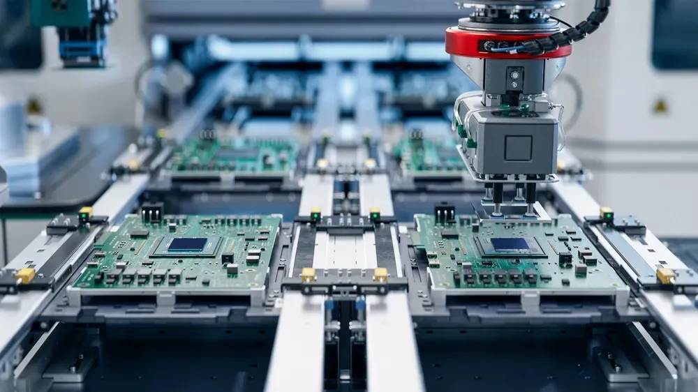
Wire-Bondable Soft Gold PCB: Surface Finish for Bond Reliability
Wire bonding joins a bare die to a board with fine metal wire, usually gold or aluminium. The joint is formed by heat, pressure and ultrasonic energy rather than by solder, and the reliability of that joint depends almost entirely on what the pad surface is made of.
A soft gold PCB finish exists to make that joint possible. Hard gold, which is excellent for connectors and edge fingers, is deliberately alloyed with cobalt or nickel and is too brittle and too contaminated for bonding. The two finishes are not interchangeable.
Why Bonding Needs Its Own Finish
Bonding forms an intermetallic layer between the wire and the pad metallisation. That layer is necessary for a strong joint, but it grows with time and temperature, and a layer that becomes too thick embrittles the interface and eventually causes a lift-off failure.
The finish must therefore be soft, pure and thin. Softness allows the wire and the pad to deform together under bonding force, producing a large contact area. Purity keeps contaminants out of the intermetallic, and controlled thickness limits how much intermetallic can form.

ENEPIG: The Standard Stack
ENEPIG stands for electroless nickel, electroless palladium, immersion gold. A nickel layer provides the barrier and the mechanical base, palladium prevents nickel from diffusing into the gold, and a thin gold layer provides the bonding surface and protects the palladium from oxidation.
Typical thicknesses are 3 to 6 microns of nickel, 0.05 to 0.1 micron of palladium and 0.03 to 0.1 micron of gold for bonding applications. The gold is deliberately thin, because thick gold makes the joint more expensive and adds a weak interface rather than a stronger one.
The palladium layer is what distinguishes ENEPIG from electroless nickel immersion gold. Without it, nickel diffuses into the thin gold layer during storage and bonding, and the bond fails at a temperature and time that cannot be predicted from the as-built sample.
Gold Thickness: Thin Is Not Cheap, It Is Correct
Gold thickness on a soft gold PCB is counterintuitive. More gold does not mean a better bond; when the gold layer is thick, the wire sits on a column of soft metal that deforms without reaching the underlying metallisation, and the joint is weaker.
Thin gold also reduces cost, because gold is the most expensive part of the stack. This is one of the few cases where the technically correct choice is also the cheaper one, provided the plating line can control thickness tightly.
Control is the hard part. Immersion gold deposits by displacement, which is self-limiting, but the thickness still varies with palladium condition, bath age and surface area. Thickness is verified by X-ray fluorescence on coupons placed on the production panel.
Nickel and Palladium Quality
The nickel layer carries the mechanical load of the bond. It must be dense, ductile and free of the black pad phenomenon, which occurs when the nickel surface is over-etched before immersion gold and the gold deposits onto a corroded surface.
Black pad produces a bond that forms correctly in the lab and fails during thermal cycling, because the joint is attached to a brittle layer rather than to solid nickel. It is a process defect that cannot be detected by a pull test at incoming inspection.
Palladium thickness is equally important. Too thin and it does not block diffusion; too thick and it becomes a hard layer that resists deformation and weakens the bond.
Bonding Process Interaction
Bonding parameters are set by the wire bonder, but the finish determines the process window. A plated pad with a uniform, clean gold surface accepts a wide range of force and ultrasonic power settings, while a contaminated surface accepts almost none.
Surface cleanliness before bonding is critical. Fingerprints, flux residue and plating salts on the pad all reduce bond strength, and a board that has been handled carelessly will show poor bond pull results that are attributed to plating.
Storage also matters. Soft gold does not oxidize, but contamination from packaging, outgassing of adhesives and atmospheric sulfur compounds can still degrade the surface. Sealed packaging with desiccant and a defined shelf life is normal practice.
Bond Testing and Acceptance
Bond quality is verified destructively and non-destructively. Wire pull testing measures the force required to break the loop, and ball shear testing measures the force required to push a ball bond off the pad.
Acceptance criteria depend on the wire diameter and the application, and they are usually agreed before production rather than applied retrospectively. The distribution of results matters as much as the minimum value, because a process drifting toward its limit produces field failures long before the minimum is reached.
Design Rules for Bondable Boards
Bond pads need to be large enough for the bonder to place a ball reliably, and they must be separated from adjacent traces so that the plating current is uniform. Plating thickness varies with the surface area of the connected copper, so a pad connected to a large plane plates differently from an isolated one.
Plating bars and current thieves are used to equalise deposit thickness across the panel. Their layout is part of the design, and the fabricator needs to know which nets are bondable so that the plating connection can be planned.
Cost Comparison and Selection
ENEPIG costs more than electroless nickel immersion gold and considerably more than hot air solder levelling, and the difference increases with the control required on gold thickness. Where bonding is required, that cost is part of the technology rather than an option.
Where a board must both bond a die and accept soldered components, ENEPIG supports both, which is why it is common in mixed assemblies. Hard gold remains the right choice for card edge contacts, and the two finishes are often used on different areas of the same board.
Further reading: electroplating additives, copper plating defect prevention, and PCB design quality characteristics.
Storage, Handling and Shelf Life
Bondable surfaces are sensitive to contamination rather than to oxidation. Packaging materials that outgas, adhesives that release organic compounds and sulfur in the atmosphere all degrade a gold surface that looks perfect under a microscope.
Handling rules follow. Gloves are mandatory, boards are stored in sealed bags with desiccant, and a defined shelf life is applied after which the surface is either re-verified or rejected. These rules are part of the specification, not workshop preference.
Process Control at the Plating Line
Bath chemistry, temperature and immersion time determine the deposit, and each of them drifts over a production run. Plating thickness is measured by X-ray fluorescence on coupons and the results are recorded against the lot.
Where bonding is critical, the fabricator should also control the nickel surface before gold deposition, because that interface, not the gold, determines whether the joint survives thermal cycling.
FAQ
Can hard gold be used for wire bonding? Not reliably. The cobalt or nickel alloyed into hard gold makes it brittle and introduces contaminants into the bond interface, which reduces pull strength and causes unpredictable failures.
How thick should the gold be for bonding? Typically 0.03 to 0.1 micron over palladium. Thicker gold weakens the joint by letting the wire deform without reaching the underlying metallisation, and it increases cost.
What is black pad and why does it matter? It is a corrosion of the nickel surface before gold deposition, producing a brittle interface that passes initial tests and fails after thermal cycling. It is a plating process defect, so supplier control is the only real protection.