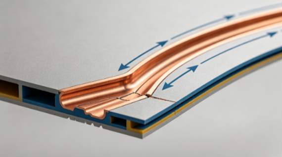
A V-Cut that is cut too deeply can significantly weaken a PCB panel and increase the risk of cracking, warpage, or edge damage during SMT assembly and reflow.
When a PCB develops cracks after reflow, the problem is not necessarily caused by soldering temperature alone. In some cases, the root cause is the mechanical weakness created by the V-Cut itself. Excessive V-Cut depth reduces the remaining material thickness and creates a geometric stress concentration along the groove.
During thermal cycling, depanelization, component mounting, and handling, this weakened region can experience combined tensile, shear, and bending stresses.
This is why V-Cut depth should be considered a mechanical-design parameter rather than simply a panelization setting.
How V-Cut Depth Creates Mechanical Stress Concentration
A V-Cut introduces a controlled groove into the PCB to facilitate depanelization. The groove reduces the cross-sectional area of the board and therefore lowers its local mechanical strength.
The remaining material at the bottom of the V-Cut acts as the structural bridge connecting the individual PCB units.
When this remaining thickness becomes too small, the local section becomes more susceptible to:
- Bending stress
- Tensile stress
- Shear stress
- Local delamination
- Resin cracking
- Glass-fiber damage
- Copper-to-laminate separation
The smaller the remaining thickness, the greater the local stress concentration can become for a given external load.
However, there is no universal V-Cut depth that is suitable for every PCB. The appropriate value depends on board thickness, laminate construction, copper distribution, panel dimensions, V-Cut geometry, blade condition, and the mechanical requirements of the assembly process.
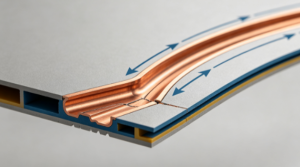
Thermal Expansion Makes the Weak Region More Sensitive
During reflow, the PCB is exposed to substantial temperature changes.
FR-4 laminate and copper have different coefficients of thermal expansion (CTE). Copper has a relatively low in-plane CTE, while the resin system has significantly different expansion behavior, particularly in the Z-axis.
When the PCB is heated, different materials attempt to expand at different rates. The multilayer structure and copper distribution constrain this movement, generating internal mechanical stress.
A V-Cut creates a geometric discontinuity where the remaining laminate thickness is reduced.
Consequently, thermal expansion does not necessarily produce uniform stress across the entire board. A portion of the deformation can become concentrated around the V-Cut groove.
This does not mean that the V-Cut itself always causes cracking during reflow. Instead, it reduces the mechanical margin of the panel and can make the region more sensitive to thermal and mechanical loading.
Remaining Thickness Is More Important Than V-Cut Depth Alone
When evaluating V-Cut depth, engineers should not consider the groove depth in isolation.
The more meaningful parameter is the remaining thickness:
Remaining thickness = Total PCB thickness − Effective V-Cut depth
The actual calculation should account for the V-Cut geometry and whether the board is cut from one or both sides.
For example, a 0.6 mm groove depth can have very different mechanical consequences on a 1.0 mm board and a 1.6 mm board.
The remaining bridge thickness should therefore be specified according to the PCB manufacturer’s process capability and the mechanical strength required for assembly and depanelization.
V-Cut Can Affect Multilayer PCB Structures
For multilayer boards, the V-Cut location must be reviewed together with the PCB stackup.
If the groove penetrates deeply enough to approach or expose internal copper structures, it may influence:
- Internal trace clearance
- Plane integrity
- Dielectric thickness
- Copper-to-edge spacing
- Local mechanical stiffness
- Laminate integrity
The V-Cut should therefore be positioned away from sensitive internal structures whenever possible.
It is also important to distinguish the mechanical effects of a V-Cut from those of a blind or buried via structure. A V-Cut does not inherently cause a “PI failure”; rather, the principal concern is local reduction in laminate cross-section and the resulting mechanical and thermal stress concentration.
V-Cut and Copper Distribution
Copper balance can also influence the behavior of a PCB panel during thermal processing.
Large copper planes, dense routing areas, and asymmetric copper distributions can cause differences in thermal expansion and mechanical stiffness across the board.
When such an area is located close to a V-Cut, the combination of:
uneven copper distribution + reduced local thickness + thermal expansion
may increase deformation or stress concentration.
Therefore, V-Cut review should not be separated from panel-level copper balancing and PCB design.
For high-density multilayer boards, engineers should review the V-Cut position together with:
- Large copper planes
- Ground and power layers
- High-density BGA areas
- Heavy copper regions
- Internal cutouts
- Board-to-board connectors
- Sensitive components near the depanelization edge
Mechanical Stress During Depanelization
Reflow is not the only process that can expose a weak V-Cut structure.
Mechanical loading during depanelization can be even more significant.
If an operator, fixture, router, or automated depaneling machine applies excessive bending force to the panel, the V-Cut becomes the preferred fracture path.
If the groove is too deep, the panel may separate with relatively low force but generate uncontrolled cracking around the groove.
If the groove is too shallow, excessive force may be required for depanelization, potentially transferring stress into nearby components or solder joints.
The engineering objective is therefore to establish a controlled balance between:
panel rigidity before depanelization and predictable separation force during depanelization.
V-Cut Depth Selection by Board Thickness
Rather than applying one fixed formula to all PCBs, manufacturers should establish a qualified V-Cut process window for each board construction.
As a general engineering approach:
- Thin PCBs: excessive groove depth can leave very little structural material and increase handling sensitivity.
- Standard-thickness PCBs: the remaining bridge thickness should be sufficient to withstand panel handling, reflow, transport, and depanelization.
- Thick multilayer PCBs: deeper or double-sided V-Cuts may be considered when appropriate, but the internal stackup and copper distribution must be reviewed.
- Rigid or heavy-copper structures: additional mechanical analysis may be required because the copper distribution can significantly change local stiffness.
For example, a V-Cut specification for a 1.6 mm PCB should not automatically be transferred to a 2.0 mm, 2.4 mm, or heavy-copper multilayer board.
The final V-Cut depth and remaining thickness should be confirmed through the manufacturer’s fabrication capability and mechanical validation.
Double-Sided V-Cut vs Single-Sided V-Cut
For thicker PCBs, a double-sided V-Cut can sometimes provide a more balanced groove structure than an excessively deep single-sided V-Cut.
A double-sided configuration may distribute the removed material between the two surfaces and reduce the amount of material that must be removed from one side.
However, double-sided V-Cut does not automatically guarantee lower stress.
Its effectiveness depends on:
- Groove angle
- Groove depth on each side
- Remaining core thickness
- Board thickness
- Laminate construction
- Internal copper location
- Panel geometry
- Depanelization method
Therefore, the design should be evaluated as a complete mechanical structure rather than assuming that double-sided cutting is always superior.
Three Common V-Cut Design Mistakes
1. Ignoring Moisture Before Reflow
Moisture absorbed by the PCB can increase the risk of delamination or cracking during thermal processing.
Moisture management should therefore be considered together with the applicable material handling and assembly requirements.
If a PCB has been stored outside the manufacturer’s specified environment for an extended period, appropriate moisture-control procedures should be followed before assembly.
2. Making the Panel Bridge Too Narrow
The bridge between individual PCB units must provide enough mechanical support during:
- SMT handling
- Conveyor transport
- Reflow
- Inspection
- Component mounting
- Depanelization
A very narrow bridge may allow excessive panel bending even when the V-Cut depth itself is within specification.
There is no universal minimum bridge width because the required value depends on panel size, PCB thickness, component placement, conveyor support, and depanelization method.
3. Mixing V-Cut and Mouse-Bite Features Without Mechanical Review
Combining V-Cut lines with routed slots or perforated mouse-bite structures can create complicated stress distributions.
At the transition between different separation methods, local geometry changes can act as stress concentrators.
Therefore, these transition areas should be reviewed during DFM rather than treated as independent features.
V-Cut and Component Reliability
A mechanically weak V-Cut can indirectly affect component reliability.
If the PCB bends excessively during depanelization or assembly, mechanical strain can be transferred to nearby:
- BGA solder joints
- QFN packages
- Ceramic capacitors
- Fine-pitch components
- Connectors
- Large components
For BGA devices, board bending can impose mechanical strain on solder joints even when the soldering profile itself is within specification.
This is particularly important when the V-Cut passes close to a large BGA or other mechanically sensitive component.
A useful design principle is:
Keep mechanically sensitive components and critical solder joints away from high-stress depanelization paths whenever practical.
How to Validate V-Cut Mechanical Reliability
Visual inspection alone cannot always identify an incipient crack at the bottom of a V-Cut.
A more complete validation process can include:
- Measure the actual V-Cut depth.
- Measure the remaining bridge thickness.
- Inspect the groove profile and blade condition.
- Check internal copper clearance.
- Evaluate panel bending during SMT handling.
- Measure depanelization force where necessary.
- Inspect cross-sections of qualification samples.
- Perform thermal cycling when required by the product specification.
- Check components near the V-Cut for solder-joint or pad damage.
- Compare results between different V-Cut process conditions.
For critical applications, strain-gauge testing can also be used to measure the mechanical strain transferred to the PCB during depanelization.
This provides more useful information than relying only on a nominal V-Cut depth.
Blade Wear and Process Control
V-Cut quality depends not only on the programmed cutting depth but also on the condition of the cutting tool.
Blade wear, machine setup, panel thickness variation, fixture condition, and material construction can all affect the actual groove geometry.
Therefore, PCB manufacturing control should include periodic verification of:
- Actual groove depth
- Remaining thickness
- Groove angle
- Edge quality
- Burr formation
- Tool wear
- Separation force
The frequency of tool inspection should be established using actual process capability and historical wear data rather than assuming a universal distance such as a fixed number of meters.
Statistical process control can be useful for identifying gradual changes before they result in production failures.
A Practical DFM Checklist for V-Cut Design
Before releasing a panel design, engineers can review the following:
Mechanical
- Is the remaining thickness sufficient?
- Is the panel rigid enough for SMT handling?
- Is the depanelization force acceptable?
Electrical
- Is there adequate copper-to-edge clearance?
- Does the V-Cut approach internal traces or planes?
- Are sensitive high-speed or power structures affected?
Assembly
- Are BGA and other sensitive components sufficiently separated from the V-Cut?
- Can the panel pass through the SMT line without excessive bending?
- Is the depanelization method compatible with the board structure?
Manufacturing
- Can the supplier achieve the specified V-Cut depth consistently?
- Is tool wear monitored?
- Has the V-Cut profile been validated on production-representative material?
How Kingda Can Help Optimize V-Cut Design
At Kingda, V-Cut optimization should be considered as part of the complete PCB design-for-manufacturing process rather than as an isolated panelization operation.
By reviewing PCB thickness, stackup, copper distribution, internal clearances, V-Cut geometry, component placement, assembly handling, and depanelization requirements together, engineers can establish a more robust manufacturing window.
The key principle is:
V-Cut depth should not be selected simply to make depanelization easier. It must provide sufficient mechanical strength during PCB manufacturing and assembly while allowing controlled separation at the end of the process.
For high-density and multilayer PCBs, early DFM review and physical validation can help identify stress-sensitive V-Cut structures before they become assembly or field-reliability problems.