Practical Notes on VIPPO
VIPPO is one of those manufacturing terms that appears on a stackup drawing without explanation and then decides whether a dense BGA can be assembled reliably. The acronym stands for via-in-pad plated over, and it describes a specific sequence: a via is placed inside a component pad, filled with solid copper, and then plated and planarized so the pad surface is flat again. It exists because putting a via in a pad solves one problem, routing density, and creates another, which is that an open hole under a solder ball wicks solder away during reflow.
What the Process Actually Is
Three things happen in sequence. The via is drilled and plated as usual, then filled with copper by an electroplating process that closes the hole from the inside out. The filled via is then ground or polished flush with the surrounding copper, and the pad surface is plated again to a controlled thickness. The result is a pad that looks and behaves like solid copper, with the via hidden inside it.
A via-in-pad plated over structure is therefore not just a filled via. The planarization and the final plating are what make the pad usable for assembly, and a supplier that fills vias without controlling flatness will produce boards that pass cross-section and still fail at placement.
Why Via-in-Pad Is Used at All
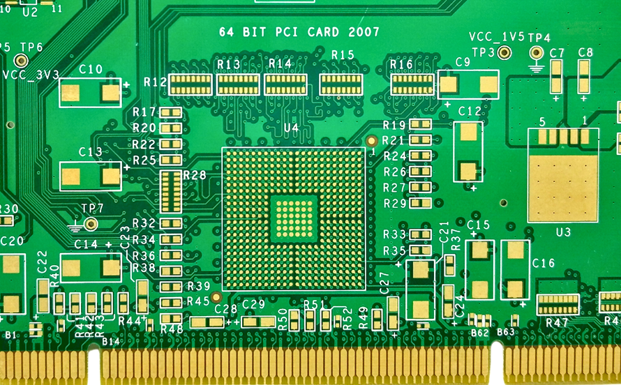
The driver is escape routing. A fine-pitch BGA presents a grid of pads at 0.4 to 0.8 mm pitch, and there is not enough room between them to route a trace out of every ball. Putting a via directly in the pad frees the channel between pads for the traces that do need to leave, which raises the achievable routing density and can remove a layer from the stackup. It also shortens the connection from the ball to the inner layers, which matters at high signal rates.
The Problem with an Unfilled Via in a Pad
An open via inside a pad acts as a drain. During reflow the paste liquefies and part of it flows down the barrel, leaving a partially filled joint, a void, or in the worst case an open connection. The pad surface is also uneven, so the ball or the paste deposit sits at an angle, which reduces placement yield on a component where every joint has to be good.
Resin plugging solves the flatness problem well enough for many designs, but it leaves a non-conductive plug in the barrel. That is acceptable electrically in most cases, and it is cheaper, but it does not help thermal transfer and it is not the same process as VIPPO.

Manufacturing Steps and Process Control
The sequence runs from high-accuracy drilling, either mechanical or laser depending on the diameter, through desmear to remove resin smear from the barrel, then copper filling by electroplating. Filling is the difficult step: the plating chemistry has to deposit preferentially at the bottom of the hole so that it closes without leaving a seam or a void in the centre. After filling, the panel is ground or polished to bring the copper flush with the surface, and the pad is plated again to reach its final thickness.
Inspection is by optical means for surface defects and by microsection for the filled barrel. A cross-section that shows an internal void is a failure even if the surface looks perfect, because the void can open during thermal cycling. Process control therefore centres on the plating chemistry, the current profile, and the consistency of the grind.
Design Rules
Keep the via diameter small relative to the pad, so there is enough annular copper for the fill to anchor to, and keep the aspect ratio comfortably inside the proven range. The filled and plated pad adds thickness, so the pad geometry has to account for it. Standard references are IPC-6012 for the finished board and IPC-4761 for via protection types, and the two together define what filled and plated over mean in acceptance terms. Confirm the interpretation with the fabricator before release, because a design that specifies a filled via and a design that specifies VIPPO are not the same order, and the documentation has to make the difference explicit. The via-in-pad and plated-through comparison is a useful starting point when deciding which structure a given pad actually needs.
Where It Is Used
VIPPO appears wherever a fine-pitch BGA has to be routed on a dense board: HDI multilayer designs, high-speed networking and computing boards, and automotive and medical assemblies where a single joint failure is expensive. It is also common where thermal transfer through the ball is important, because a solid copper plug conducts heat into the inner layers far better than a resin plug or an open barrel.
It is not needed on every BGA. A coarse-pitch package on a board with routing room can use conventional vias placed outside the pads, and the extra process cost buys nothing. The decision belongs to the escape routing analysis, not to habit. Where the design does need to stack vias across several layers, the blind and buried via stack selection rules cover how the structures combine.
Electrical and Thermal Effects
The electrical benefit is mostly about the stub effect. A through via that continues past the layer it serves leaves an unterminated stub, and that stub resonates at high frequency, degrading the signal. A filled via that stops where it is needed removes the stub, which is why VIPPO and stacked microvia structures are common on fast interfaces. The thermal benefit comes from the copper itself: a solid plug carries heat from the ball into the inner layers, where it can spread.
Cost
VIPPO adds cost because it adds process steps and reduces yield during ramp. Reference pricing runs roughly 120 to 250 dollars per square metre for a four-layer HDI prototype, 220 to 420 for a six-layer board with dense BGA routing, and 380 to 750 for an eight- or ten-layer high-speed board. The main variables are layer count and thickness, the number and density of the plated-over vias, and the precision the fill process has to hold. Against that, the process usually reduces system-level rework and field failure, and it can remove a routing layer, which is where the economic argument usually lands.
Choosing a Supplier
Four questions separate capable suppliers. Does the line have its own copper filling capability, or does it subcontract the step? Can it provide cross-section evidence of void-free fill on a coupon? Does it work to IPC-6012 and IPC-4761 acceptance criteria, and does it state which via protection type it is delivering? And does it offer design review before the stackup is frozen, since a small change to via diameter or pad size can move the design into a much easier process window. The same questions apply to any HDI fabrication and CAM capability, and the answers are more informative than a capability list.
FAQ
What does VIPPO stand for? Via-in-pad plated over. The via sits inside the component pad, is filled with solid copper, and is planarized and plated so the pad surface is flat.
Does every BGA design need VIPPO? No. Coarse-pitch packages with routing room can use vias placed outside the pads. Fine-pitch and high-reliability designs usually benefit.
How is it different from resin plugging? Resin plugging fills the barrel with a non-conductive material and caps it. VIPPO fills with copper, which improves both current capacity and heat transfer, and it holds tighter flatness.
Is the extra cost justified? It usually is when the alternative is an additional routing layer or a placement yield problem. On a coarse-pitch board with room to spare, it is not.