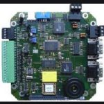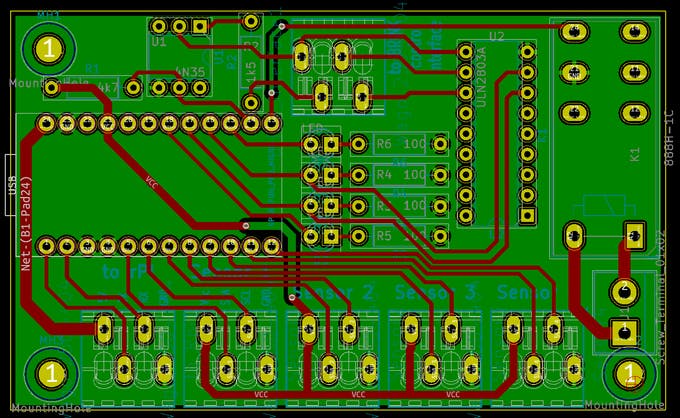
In modern electronic systems, High-Speed PCB Design plays an increasingly important role in achieving fast, stable, and reliable data transmission. As data rates continue to increase and electronic products become smaller and more highly integrated, PCB designers must pay greater attention to Signal Integrity, power distribution, routing topology, impedance, crosstalk, and electromagnetic interference.
High-speed design is not determined solely by the nominal operating frequency of a digital signal. The rise time and fall time of the signal are often more important factors. Even a relatively low-frequency digital signal can create high-speed transmission-line effects when its edge rate is sufficiently fast.
For this reason, high-speed PCB design requires careful planning from the early stages of schematic development and component placement through PCB routing, simulation, verification, and manufacturing.
What Is High-Speed PCB Design?
High-speed PCB design refers to the design methodology used when high-speed digital signals or other fast-changing electrical signals are transmitted between components.
There is no single universal frequency threshold that defines a high-speed PCB. Instead, designers typically evaluate factors such as signal rise time, trace length, propagation delay, operating frequency, and the electrical characteristics of the interconnect.
Modern high-speed PCBs may contain high-speed digital interfaces, memory buses, processors, high-speed serial links, wireless communication circuits, and RF front-end modules. These systems require controlled electrical characteristics throughout the signal path.
The main objectives of High-Speed PCB Design include:
- Maintaining Signal Integrity
- Controlling transmission-line impedance
- Reducing signal reflection and crosstalk
- Minimizing timing skew and propagation delay
- Improving Power Integrity
- Reducing electromagnetic interference
- Ensuring reliable PCB manufacturing and assembly
Planning the PCB Stackup and Impedance
The PCB Stackup is one of the most important factors affecting high-speed signal performance. A properly designed stackup provides stable reference planes, controlled impedance, shorter return paths, and better power distribution.
When developing a high-speed stackup, designers should consider the following factors.
1. Board Size and Number of Nets
The physical dimensions of the PCB and the number of electrical nets determine how much routing space is available. A larger board may provide more routing space, while a compact board may require additional signal layers.
2. Routing Density
High component density and a large number of high-speed nets can significantly increase routing difficulty. Additional internal signal layers may be required to achieve appropriate spacing and routing topology.
3. Interface Distribution
High-speed interfaces should be planned carefully. Keeping related signals on the same layer can help maintain consistent impedance and reduce timing differences.
4. Low-Speed and RF Signals
A PCB may contain both high-speed digital signals and lower-speed or RF circuits. Sensitive analog and RF sections should be appropriately separated from noisy high-speed digital circuits to minimize interference.
5. Power and Ground Planes
A reliable power distribution structure is essential for high-speed systems. Dedicated power and ground planes can provide low-impedance return paths and support stable operation of high-speed devices.
High-Speed PCB Routing Design Guidelines
1. Routing Strategy
High-Speed Routing should begin with critical signals rather than non-critical connections.
Clock signals, differential pairs, memory buses, high-speed serial interfaces, and other sensitive nets should receive priority during routing.
Designers should minimize unnecessary vias, sharp direction changes, excessive trace length, and long parallel routing sections.
Interactive routing is often preferred for critical signals because it gives designers greater control over trace geometry and signal paths. Automatic routing can be used for less critical connections after important routing constraints have been established.
2. Power and Ground Design
Good Power Integrity is closely related to high-speed signal performance.
Decoupling capacitors should be placed as close as practical to the power pins of integrated circuits. Short connections between the capacitor, power pin, and ground plane help reduce parasitic inductance.
Large and continuous ground planes are also important because they provide low-impedance return paths for high-frequency currents.
Instead of relying only on wider traces, designers should consider the complete power distribution network, including planes, vias, capacitors, and component placement.
3. Digital and Analog Ground Management
Digital circuits can generate significant switching noise, while sensitive analog circuits may be more susceptible to interference.
Therefore, PCB layout should separate noisy digital sections from sensitive analog sections where appropriate. High-speed signals should be kept away from sensitive analog components and critical analog routing.
However, simply splitting ground planes is not always the best solution. The return-current path and actual circuit architecture should be evaluated before deciding how to implement ground segmentation.
4. Signal Layer and Reference Plane Selection
High-speed signal traces should normally be routed over a continuous reference plane.
A stable reference plane provides a predictable return-current path and helps maintain controlled impedance. If a high-speed trace changes layers, the return path should also be considered carefully.
Ground vias can be used near signal vias when necessary to help maintain return-current continuity.
5. Differential Pair Routing
A Differential Pair consists of two complementary traces carrying related signals.
Differential routing is widely used in high-speed interfaces because it can provide improved noise immunity and reduce common-mode interference when properly designed.
The two traces should generally maintain consistent spacing, length, reference-plane conditions, and routing geometry. Unnecessary separation or asymmetrical routing can increase skew and degrade signal performance.
6. Large Copper Areas
Large copper areas can improve power distribution and thermal performance, but their connection to component pads must be designed carefully.
Thermal relief structures are often used when connecting component pads to large copper planes. This can help improve soldering consistency during PCB assembly.
Impedance Control in High-Speed PCB Design
Impedance Control is a critical part of modern high-speed PCB design.
Common controlled-impedance configurations include approximately 50-ohm single-ended routing and approximately 100-ohm differential routing, although actual target values depend on the interface and system requirements.
Other impedance values may also be required for specific applications.
The controlled impedance of a PCB trace is affected by several parameters, including:
- Trace width
- Copper thickness
- Dielectric thickness
- Dielectric constant
- Distance to the reference plane
- Trace geometry
- PCB material structure
Therefore, impedance should not be determined by trace width alone.
The target impedance should be established during the stackup design stage. PCB designers and manufacturers should work together to confirm material selection, dielectric thickness, copper thickness, and manufacturing tolerances.
Signal Integrity and Simulation
Signal Integrity analysis becomes increasingly important as signal speeds increase.
Before routing, designers can use simulation tools to evaluate critical interfaces and determine suitable routing constraints.
Simulation can help identify potential problems such as:
- Signal reflection
- Overshoot and undershoot
- Crosstalk
- Excessive insertion loss
- Timing problems
- Impedance discontinuities
- Ground bounce
After routing, post-layout simulation can be used to verify whether the actual PCB meets the expected electrical requirements.
This design-and-verify process helps reduce the risk of expensive redesigns and improves overall product reliability.
Design Rule Check and Manufacturing Considerations
A comprehensive Design Rule Check (DRC) should be performed before releasing the PCB for manufacturing.
The review should cover trace width, spacing, via size, differential-pair requirements, impedance constraints, copper clearance, power and ground structures, and other critical design parameters.
For high-speed PCBs, electrical performance and manufacturing capability must be considered together. A design may theoretically provide excellent signal performance but still be difficult or expensive to manufacture if its trace widths, spacing, drilling requirements, or stackup tolerances exceed the manufacturer’s capabilities.
Kingda can evaluate high-speed PCB designs from both electrical and manufacturing perspectives, helping customers balance Signal Integrity, Impedance Control, reliability, manufacturability, and production cost.
Conclusion
High-Speed PCB Design is a systematic engineering process rather than simply increasing routing density or using narrower traces. Successful high-speed PCB development requires coordinated control of the PCB Stackup, High-Speed Routing, Power Integrity, Signal Integrity, and Impedance Control.
From component placement and reference-plane selection to differential-pair routing, impedance verification, simulation, and Design Rule Check (DRC), every stage can affect the final electrical performance of the PCB.
As electronic products continue to move toward higher data rates, smaller form factors, and greater integration, high-speed PCB design will require increasingly precise materials, manufacturing processes, simulation tools, and design methodologies. With professional engineering and manufacturing support, Kingda can help customers develop reliable high-speed PCB solutions while maintaining a practical balance between performance, manufacturability, and cost.