5G Base Station High-Frequency PCB Supplier
As 5G networks continue to expand and communication technologies evolve, the performance and deployment efficiency of 5G base stations increasingly depend on high-performance electronic components. Among these components, the 5G Base Station PCB serves as a critical platform for RF signal transmission, power distribution, control circuits, and antenna-related electronics.
The quality and manufacturing capability of a High-Frequency PCB Supplier can directly affect signal integrity, product reliability, production efficiency, and delivery stability. For communication equipment manufacturers, selecting a supplier with advanced materials, precision fabrication capabilities, and reliable engineering support is essential for developing and scaling 5G infrastructure products.
The Role of High-Frequency PCBs in 5G Base Stations
A High-Frequency PCB is designed to handle high-frequency and high-speed signals while maintaining predictable electrical performance. In 5G base stations, these circuit boards can be used in radio-frequency modules, antenna systems, transceiver units, signal-processing circuits, and other communication subsystems.
Compared with conventional FR-4 circuit boards, high-frequency PCB structures typically require greater control over dielectric properties, copper geometry, layer construction, and impedance. These factors influence insertion loss, signal attenuation, phase stability, and overall signal integrity.
For demanding communication applications, PCB fabrication must therefore consider electrical performance together with mechanical reliability and manufacturability.
GOPCBA provides advanced PCB Manufacturing Services covering multilayer, HDI, high-frequency, high-speed, controlled-impedance, and other specialized PCB technologies.
Why High-Frequency PCB Technology Matters for 5G
5G communication equipment operates with increasingly demanding requirements for bandwidth, transmission speed, signal density, and system integration. As signal frequencies and data rates increase, PCB geometry becomes an important part of the electrical design.
A suitable 5G Base Station PCB needs to maintain stable transmission characteristics while controlling losses and impedance variations. Small changes in trace width, copper thickness, dielectric thickness, or layer registration can influence transmission-line behavior.
For this reason, a qualified High-Frequency PCB Supplier should be capable of combining material selection, stack-up engineering, precision fabrication, and electrical testing into a consistent manufacturing process.
Core Capabilities of a 5G Base Station High-Frequency PCB Supplier
High-Performance Material Selection
Material selection is one of the most important factors in high-frequency PCB manufacturing.
A professional supplier should be able to select materials according to frequency, loss requirements, thermal conditions, mechanical constraints, and production requirements. Depending on the application, high-frequency PCB projects may use specialized low-loss laminates from manufacturers such as Rogers, Taconic, Arlon, Isola, Panasonic, or other qualified material suppliers.
Low-loss dielectric materials can help reduce signal attenuation, while stable dielectric properties can improve impedance consistency and signal performance.
Material selection should also consider production availability. A material that performs well in prototypes may not always be the most practical choice for long-term volume production. Therefore, the material strategy should be evaluated together with the complete manufacturing process.
Precision Multilayer PCB Manufacturing
5G communication equipment often requires complex multilayer structures to accommodate high routing density, RF circuits, power distribution, grounding, and signal-processing functions.
A reliable Multilayer PCB manufacturing process requires accurate layer registration, controlled dielectric thickness, stable lamination, precise drilling, and reliable plating.
For high-speed and high-frequency applications, the PCB stack-up should be developed with electrical requirements in mind. Important factors include:
- Layer arrangement
- Dielectric thickness
- Copper thickness
- Dielectric constant
- Reference-plane location
- Controlled impedance
- Via structure
- Thermal requirements
GOPCBA supports advanced multilayer PCB manufacturing and high-density PCB structures for demanding electronic applications.
Controlled Impedance and Signal Integrity
Controlled impedance is essential for many high-frequency communication circuits.
The impedance of a transmission line is influenced by trace width, copper thickness, dielectric thickness, dielectric constant, reference-plane distance, and other physical parameters. Manufacturing variations in these dimensions can cause impedance deviations and affect signal quality.
A capable supplier should therefore provide engineering support before production and verify that the final PCB construction matches the intended electrical design.
GOPCBA provides Controlled Impedance PCB manufacturing capabilities for high-speed and high-frequency applications, with engineering support for stack-up evaluation and manufacturing feasibility.
HDI, Blind and Buried Via Technology
As 5G equipment becomes smaller while incorporating more functions, routing density continues to increase. HDI technology can provide additional routing channels while reducing the space occupied by conventional through-hole vias.
Microvias, blind vias, buried vias, and sequential lamination can be used according to the board structure and electrical requirements.
GOPCBA’s HDI PCB Manufacturing capabilities support high-density interconnect structures, microvias, blind and buried vias, and advanced multilayer designs.
HDI can be particularly useful for compact communication modules, fine-pitch components, high-density RF systems, and applications where conventional through-hole technology cannot provide sufficient routing efficiency.
Reliable Manufacturing and Quality Control
5G base stations are often deployed in demanding environments and may be expected to operate continuously for long periods. PCB reliability is therefore not limited to initial electrical performance.
A reliable manufacturing process should control:
- Lamination parameters
- Layer registration
- Drilling accuracy
- Copper plating
- Etching quality
- Solder mask
- Surface finish
- Impedance
- Electrical performance
- Final inspection
Production consistency is especially important when a communication equipment design moves from engineering samples to volume production.
Manufacturing Requirements for 5G Base Station PCBs
Low-Loss Signal Transmission
High-frequency signals are sensitive to dielectric and conductor losses. Selecting suitable low-loss materials and controlling transmission-line geometry can help reduce attenuation and preserve signal quality.
The PCB stack-up should be designed according to the actual frequency range, impedance requirements, routing structure, and system architecture rather than relying on a standard construction.
Thermal and Mechanical Stability
5G base stations may operate continuously and can generate considerable heat. PCB materials and construction must therefore provide sufficient thermal and dimensional stability for the intended operating environment.
Material selection, copper distribution, thermal vias, board thickness, and mechanical construction should be evaluated together.
Precise Layer Registration
Complex multilayer and HDI PCBs require accurate registration between copper layers, dielectric materials, vias, and component locations.
Poor registration can affect routing accuracy, impedance, via connectivity, and assembly reliability. Precision lamination and controlled manufacturing parameters are therefore critical for advanced communication PCBs.
Prototype-to-Production Support
5G hardware development often involves multiple engineering iterations before entering volume production. A manufacturing partner should be able to support the complete transition from prototype validation to production.
GOPCBA provides PCB Prototype Manufacturing and production manufacturing support, allowing engineers to validate PCB performance before scaling to larger quantities.
Why Choose GOPCBA for 5G High-Frequency PCB Manufacturing?
GOPCBA provides PCB manufacturing and PCBA services for demanding applications including telecommunications, AI computing, industrial automation, energy systems, and other high-performance electronics.
Its manufacturing capabilities cover high-frequency PCB, high-speed PCB, multilayer PCB, HDI PCB, controlled-impedance PCB, high-TG PCB, rigid-flex PCB, heavy-copper PCB, and other advanced PCB technologies.
For communication equipment manufacturers, GOPCBA can support the development process from engineering review and PCB prototyping through PCB fabrication and assembly.
The company also provides PCB Design and Layout Services covering high-frequency, high-speed, multilayer, HDI, impedance-controlled, and mixed-signal PCB designs. Early engineering involvement can help identify stack-up, signal-integrity, and manufacturability issues before production.
5G Base Station PCB Manufacturing: From Design to Production
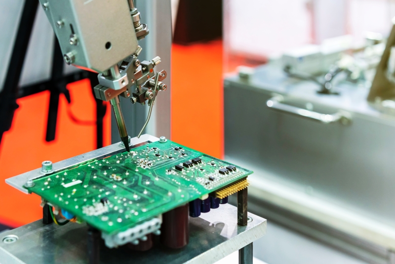
A successful 5G Base Station PCB project requires cooperation between PCB design, material engineering, fabrication, and assembly teams.
A typical development process includes:
- Electrical and mechanical requirement analysis
Determine frequency range, signal requirements, board dimensions, layer count, thermal conditions, and reliability targets. - Material selection
Select appropriate high-frequency or high-speed laminate according to electrical and mechanical requirements. - Stack-up development
Define layer arrangement, dielectric thickness, copper thickness, reference planes, and impedance requirements. - DFM and engineering review
Review trace geometry, via structures, spacing, manufacturability, and material availability. - Prototype manufacturing
Produce engineering samples for electrical, mechanical, thermal, and functional validation. - Testing and verification
Verify impedance, signal integrity, dimensional accuracy, electrical connectivity, and other project-specific requirements. - Production scaling
Transfer the validated design into stable low-volume or mass production while maintaining consistent materials and process parameters.
This integrated approach helps reduce redesign risks and supports a smoother transition from prototype to production.
The Future of High-Frequency PCBs for 5G Infrastructure
As 5G networks continue to evolve toward higher bandwidth, greater network density, and more sophisticated radio architectures, PCB technology will face increasingly demanding requirements.
Future High-Frequency PCB solutions are likely to emphasize:
- Lower transmission loss
- More precise impedance control
- Higher routing density
- Advanced low-loss materials
- More complex multilayer structures
- HDI and microvia technology
- Improved thermal management
- Higher manufacturing consistency
The combination of material expertise, precision fabrication, signal-integrity engineering, and stable production will become increasingly important for communication equipment manufacturers.
Conclusion
The 5G Base Station PCB is a critical component in modern communication infrastructure. Its electrical performance, dimensional stability, thermal reliability, and manufacturing consistency can directly influence the performance of the equipment in which it is installed.
Choosing an experienced High-Frequency PCB Supplier requires more than evaluating price or production capacity. Material selection, controlled impedance, multilayer fabrication, HDI technology, precision lamination, quality control, engineering support, and prototype-to-production capability should all be considered.
GOPCBA provides advanced PCB manufacturing and PCBA solutions for high-frequency, high-speed, multilayer, HDI, and controlled-impedance applications, supporting communication equipment manufacturers from PCB development and prototyping through production and assembly.