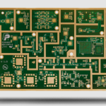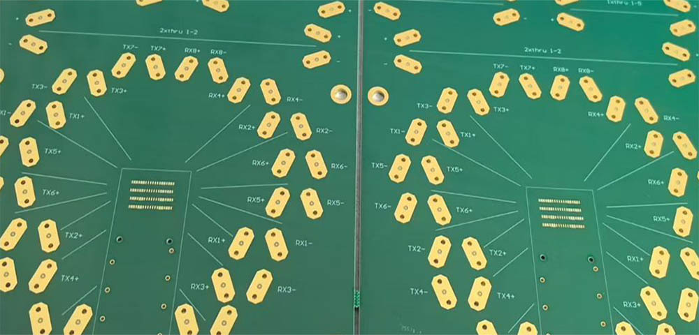
As electronic products continue to achieve higher data rates, smaller form factors, and greater integration, High-Speed PCB Design has become increasingly important. High-speed signals are more sensitive to trace geometry, reference planes, vias, impedance discontinuities, crosstalk, and power noise than conventional low-speed signals.
A PCB that works correctly at low frequencies may experience reflection, ringing, timing errors, excessive electromagnetic radiation, or transmission loss when used for high-speed applications. Therefore, designers need to consider electrical performance from the beginning of the PCB layout process rather than treating signal integrity as a final-stage problem.
The following eight routing rules can help designers build more reliable and manufacturable high-speed PCB layouts.
Rule 1: Properly Shield Critical High-Speed Signals
In High-Speed PCB Design, clock signals and other critical High-Speed Signals should be routed carefully to minimize interference from surrounding circuits.
High-speed clock traces can generate significant electromagnetic fields because of their fast rise and fall times. If these signals are routed close to sensitive analog circuits, RF sections, or other high-speed traces, unwanted coupling may occur.
A common approach is to route critical signals close to a continuous ground reference and use ground vias where appropriate to strengthen the return-current path. Ground shielding structures can also be considered when the application has strict EMI requirements.
However, shielding should not simply be implemented by placing ground vias at a fixed distance. The appropriate via spacing depends on the signal characteristics, PCB stackup, operating environment, and electromagnetic requirements.
Designers should also avoid routing high-speed signals across gaps or slots in the reference plane. A continuous reference plane is often more effective than excessive shielding structures.
Rule 2: Avoid Closed-Loop Routing
As PCB layouts become more compact and routing density increases, unnecessary loops can easily appear during routing.
A closed-loop routing structure can create a larger current loop and potentially behave like an unintended antenna. The larger the loop area, the greater the possibility of electromagnetic radiation.
For clock signals, reset signals, high-speed data lines, and other sensitive nets, designers should use direct and clearly defined routing paths whenever possible.
During layout optimization, designers should inspect not only the signal trace itself but also its corresponding Return Path. A visually short signal route can still create a large current loop if its return path is interrupted.
Therefore, minimizing both signal-path length and return-loop area is an important principle in Signal Integrity design.

Rule 3: Avoid Unnecessary Open-Loop Branches
Closed loops are not the only routing structure that can create problems. Uncontrolled branches and excessive stubs can also negatively affect high-speed signal performance.
When a high-speed signal reaches an unnecessary branch, part of the signal energy may travel down the branch and reflect back toward the main transmission path. This can result in ringing, overshoot, undershoot, and timing distortion.
For high-speed interfaces, unnecessary stubs should therefore be minimized.
If multiple devices must share the same signal, the designer should select an appropriate topology based on the interface requirements. Point-to-point routing, daisy-chain routing, fly-by structures, or carefully designed branching networks may be used depending on the application.
The correct topology should be determined by signal rise time, load capacitance, trace length, termination method, and interface specifications.
Rule 4: Maintain Continuous Controlled Impedance
Impedance Control is one of the most important elements of modern high-speed PCB design.
A high-speed transmission line should maintain a reasonably consistent impedance throughout its entire signal path. Sudden changes in trace width, dielectric thickness, reference-plane distance, or layer structure can create impedance discontinuities.
For example, when a signal transitions from one layer to another through a via, the surrounding geometry changes. If the layer transition is not properly designed, the via structure may introduce additional parasitic capacitance and inductance.
A controlled-impedance PCB therefore requires coordination between PCB designers and manufacturers.
Important parameters include:
- Trace width
- Copper thickness
- Dielectric thickness
- Dielectric constant
- Reference-plane distance
- Via structure
- PCB material
- Layer stackup
The target impedance should be established during the PCB Stackup design stage rather than being determined only after routing is completed.
Rule 5: Optimize Routing Direction Between Adjacent Layers
Routing direction is another useful consideration when designing multilayer PCBs.
If long parallel traces are routed in the same direction on adjacent signal layers, electromagnetic coupling may increase, resulting in Crosstalk.
A common layout strategy is to route predominantly in one direction on one signal layer and use a different direction on the adjacent layer. For example, one layer may primarily carry horizontal traces while the next signal layer primarily carries vertical traces.
This approach can reduce long parallel sections between adjacent layers.
However, routing direction should not be considered independently. Designers must also evaluate:
- Distance between signal layers
- Reference-plane structure
- Trace spacing
- Signal rise time
- Parallel routing length
- Dielectric material
Increasing spacing between sensitive signals is often an effective way to reduce Crosstalk.
Rule 6: Select the Correct Routing Topology
Topology plays an important role in high-speed PCB performance.
Common routing structures include point-to-point, daisy-chain, star, and fly-by topologies. Each topology has different electrical characteristics and should be selected according to the interface requirements.
For example, point-to-point routing is relatively straightforward because there are only two primary endpoints. Multi-load systems are more complicated because reflections from different branches or loads can interact with each other.
A star structure may be useful for certain applications, but it can also create multiple branches and impedance discontinuities if it is not carefully designed.
Therefore, designers should not select a topology simply because it appears convenient from a layout perspective. The signal path, load distribution, termination strategy, and transmission-line characteristics should all be evaluated.
For particularly sensitive interfaces, pre-layout simulation can help determine the most appropriate topology before PCB routing begins.
Rule 7: Consider Electrical Trace Length and Resonance
Trace length becomes increasingly important as signal edge rates become faster.
A digital signal should not be classified as high-speed only according to its clock frequency. A signal with a relatively low repetition frequency may still behave as a high-speed transmission line if its rise time is very short.
When the electrical length of a PCB trace becomes significant relative to the signal transition time or wavelength, transmission-line effects must be considered.
Long traces can introduce propagation delay and increase the possibility of reflection and resonance. Therefore, designers should evaluate critical traces based on:
- Signal rise and fall time
- Trace length
- Propagation velocity
- Operating frequency
- Load characteristics
- Termination method
Keeping critical signal paths appropriately short can help reduce unnecessary delay and signal degradation.
Rule 8: Maintain a Continuous Return Path
A reliable Return Path is essential for every high-speed signal.
High-frequency return current tends to follow the path of lowest impedance, usually flowing close to the signal trace along its reference plane.
If a high-speed signal crosses a split in the reference plane, the return current may be forced to travel around the discontinuity. This increases the effective loop area and can cause higher radiation, greater noise, and degraded Signal Integrity.
For this reason, designers should avoid routing critical high-speed traces across:
- Ground-plane gaps
- Power-plane splits
- Slots
- Large voids
- Areas with insufficient reference-plane continuity
When a signal changes layers, the return path should also be considered. Properly positioned ground vias can help maintain return-current continuity when the signal transitions between layers.
Decoupling Capacitor Placement
Although routing is important, high-speed PCB performance also depends heavily on the power distribution network.
Decoupling Capacitors should generally be placed as close as practical to the power pins of the corresponding IC.
The connection between the IC power pin, capacitor, and ground should be short and have low parasitic inductance. Long traces between the capacitor and IC can reduce the capacitor’s effectiveness at high frequencies.
For high-performance processors, FPGAs, memory devices, and communication ICs, multiple decoupling capacitors with different capacitance values may be used to address different frequency ranges.
The exact capacitor configuration should be determined according to the IC manufacturer’s recommendations and the requirements of the power distribution network.
The Importance of Simulation Before and After Routing
For complex high-speed designs, simulation should be incorporated into the PCB development process.
Before routing, engineers can perform pre-layout simulation to evaluate possible routing topologies, termination strategies, trace impedance, and signal behavior.
After routing, post-layout simulation can verify the actual PCB structure and identify potential issues such as:
- Signal reflection
- Ringing
- Overshoot and undershoot
- Timing skew
- Crosstalk
- Impedance discontinuity
- Excessive insertion loss
This combination of simulation and physical PCB design can significantly reduce the risk of discovering signal-integrity problems after manufacturing.
PCB Manufacturing Considerations for High-Speed Designs
High-speed PCB performance is closely related to manufacturing capability.
A theoretically optimized layout may still fail to achieve the expected electrical performance if manufacturing tolerances are not properly controlled.
For example, variations in copper thickness, dielectric thickness, trace width, etching, drilling, and layer registration can influence the final impedance of the PCB.
Therefore, designers should communicate controlled-impedance requirements to the PCB manufacturer before production.
Kingda can evaluate the PCB stackup, material selection, trace geometry, impedance requirements, and manufacturing tolerances during the engineering stage. This helps ensure that the high-speed PCB design is not only electrically optimized but also practical for mass production.
Conclusion
Reliable High-Speed PCB Design requires comprehensive control of routing, stackup, impedance, power distribution, and return-current paths.
The eight rules discussed above provide a practical framework for reducing EMI, Crosstalk, signal reflection, and other common high-speed PCB problems. Designers should avoid unnecessary loops and branches, maintain continuous reference planes, carefully select routing topology, control impedance, and ensure an effective Return Path for critical signals.
At the same time, Decoupling Capacitors, simulation, and manufacturing tolerances should be considered as part of the overall design strategy.
As electronic products continue to move toward higher data rates and greater integration, high-speed PCB design will require closer cooperation between design engineers and PCB manufacturers. With professional engineering support and controlled manufacturing processes, Kingda helps customers develop high-performance PCB solutions with a practical balance between Signal Integrity, reliability, manufacturability, and cost.