BGA vs LGA PCB Assembly: Key Differences, Processes, Costs, and Selection Guide
In high-density electronic product design, BGA and LGA PCB assembly are both very common packaging and interconnection solutions. BGA (Ball Grid Array) and LGA (Land Grid Array) both feature bottom array-style contact structures that enable high I/O density within a limited PCB area. They are widely used in processors, memory devices, communication modules, industrial control equipment, automotive electronics, and high-performance computing systems.
However, BGA and LGA are not identical packaging technologies. They differ significantly in soldering structure, PCB pad design, SMT placement, reflow soldering, X-Ray inspection, rework, reliability, and PCB assembly costs.
For electronic engineers and OEM procurement professionals, understanding the differences between BGA PCB assembly and LGA PCB assembly helps in selecting the more suitable packaging solution during product design, while also reducing quality risks in PCB manufacturing and electronic assembly.
This article systematically introduces the differences between BGA and LGA PCB assembly, providing a professional analysis from the perspectives of PCB design, soldering process, inspection, cost, reliability, and application scenarios.
1. What is BGA PCB Assembly?
BGA PCB assembly refers to the SMT (Surface Mount Technology) process in which a BGA (Ball Grid Array) packaged component is connected to PCB pads via an array of solder balls arranged in a grid pattern on the bottom of the component.
BGA components typically feature a dense array of solder balls on the underside. After PCB fabrication, solder paste is printed through a stencil, and a high-speed, high-precision SMT placement machine accurately positions the BGA component onto the corresponding pads. The assembly then passes through a controlled reflow oven, where the solder balls and paste melt together to form reliable electrical and mechanical connections.
A typical BGA PCB assembly process includes:
- PCB incoming inspection
- Solder paste printing
- SPI (Solder Paste Inspection)
- Precision BGA placement
- Reflow soldering
- AOI inspection
- X-Ray inspection
- Electrical testing
- Final quality inspection
Key advantages of BGA packaging include:
- High I/O pin density
- Space savings on PCB
- Supports miniaturized product designs
- Suitable for high-speed digital circuits
- Short lead lengths, helping reduce parasitic parameters for certain high-speed signals
- Well-suited for automated SMT mass production
Therefore, BGA is widely used in CPUs, GPUs, FPGAs, DDR memory, communication chips, network processors, automotive electronic controllers, and industrial control equipment.
For high-density BGA PCB assembly projects, PCB design, solder paste printing precision, placement accuracy, and reflow temperature profiles must all be tightly controlled.
Looking for professional SMT assembly services? gopcb’s SMT PCB assembly offers high-precision placement for fine-pitch BGA and LGA components.
2. What is LGA PCB Assembly?
LGA (Land Grid Array) is similar to BGA in that it uses a bottom array-style connection structure, but the key difference is that LGA components feature flat metal pads or contacts on the underside rather than solder balls.
In LGA PCB assembly, the metal contacts on the underside of the component are precisely aligned with the corresponding pads on the PCB, and connections are formed through solder paste reflow.
LGA is commonly found in:
- Processors
- Sensors
- MEMS devices
- RF modules
- Communication chips
- Industrial electronics
- Consumer electronics
- High-density ICs
LGA packaging features flatter bottom contacts without pre-formed solder balls like BGA. Therefore, PCB pad design, solder paste volume control, component coplanarity, and reflow processes must be optimized based on the specific component specifications.
3. Key Differences Between BGA and LGA PCB Assembly
The core difference between BGA and LGA lies in the bottom connection structure. In simple terms: BGA uses solder balls to connect to the PCB, while LGA uses flat metal contacts to connect to the PCB.
3.1 Component Bottom Connection Structure
BGA: Features an array of solder balls on the underside.
- Pre-formed solder balls on the component
- Solder balls participate in forming the final solder joint
- Suitable for high I/O density designs
- Enables compact package sizes
- Common in high-performance processors and memory
LGA: Features flat metal pads or contacts on the underside.
- No traditional BGA solder balls
- Solder paste on the PCB forms the soldered connection
- Dense arrangement of bottom contacts
- Suitable for high-density, miniaturized products
Therefore, when comparing BGA and LGA packaging for PCB assembly, the connection structure is the most fundamental and important difference.
3.2 PCB Pad Design
While both BGA and LGA require high-precision PCB pad design, the specific Land Pattern varies depending on component manufacturer, pin pitch, pad size, and package structure.
BGA PCB design typically considers:
- BGA pitch (solder ball spacing)
- PCB pad dimensions
- Solder mask opening
- Fanout design
- Via-in-Pad
- Microvias
- Blind vias
- Buried vias
- HDI structures
- High-speed signal routing
For ultra-fine pitch BGA components, traditional through-holes may not meet routing requirements, so HDI PCB, laser microvias, and Via-in-Pad technologies may be needed.
LGA also requires high-precision pad design, with focus on:
- LGA contact pitch
- PCB pad dimensions
- Pad spacing
- Solder mask clearance
- Trace width
- Trace spacing
- Via placement
- PCB warpage
- Component coplanarity
For both BGA and LGA, it is not recommended to simply apply generic package dimensions. Instead, priority should be given to the component manufacturer’s datasheet and recommended Land Pattern for PCB footprint design.
3.3 PCB Routing Complexity
Both BGA and LGA are high-density packages, making PCB routing a significant challenge during the design phase.
For high-pin-count BGA components, engineers typically need to perform fanout design to route the inner solder balls out layer by layer.
Common BGA fanout methods include:
- Dog-Bone Fanout
- Via-in-Pad
- Microvia
- Blind Via
- Buried Via
- HDI multi-stage structures
Especially for 0.5mm, 0.4mm, or even finer pitch BGA devices, higher PCB manufacturing capabilities are required.
LGA may also require multi-layer PCBs and HDI structures, but the difficulty depends on LGA package size, contact count, pitch, and the product’s routing requirements.
Therefore, the routing difficulty of BGA versus LGA PCB cannot be judged solely by package name; it must be analyzed based on the specific component and PCB stackup.
Need expert PCB design support? gopcb’s PCB design & layout services help you optimize fanout and routing for BGA and LGA packages.
4. BGA vs LGA Soldering Process Comparison
Both BGA and LGA generally use SMT automated placement and reflow soldering, but there are some process differences.
BGA PCB Assembly Process Flow
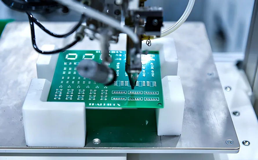
Step 1: Solder Paste Printing
Solder paste is printed onto PCB pads through a stencil. For fine-pitch BGA, strict control is needed for:
- Paste thickness
- Stencil thickness
- Stencil aperture size
- Paste release performance
- Printing offset
- Paste volume
Print quality directly affects subsequent BGA solder joint quality.
Step 2: SPI Solder Paste Inspection
SPI (Solder Paste Inspection) checks:
- Paste height
- Paste volume
- Paste area
- Print offset
- Print consistency
SPI helps detect printing anomalies before reflow.
Step 3: BGA Placement
High-precision SMT placement machines accurately position BGA components on PCB pads. For fine-pitch BGA, the equipment must have sufficient:
- X/Y positioning accuracy
- Z-axis control
- Optical recognition
- Component correction capability
Step 4: Reflow Soldering
The PCB passes through a reflow oven, where solder paste and BGA solder balls melt according to the set temperature profile to form solder joints.
The reflow profile must consider:
- PCB material
- Component temperature ratings
- Solder paste type
- PCB thickness
- Copper structure
- Thermal mass
- Lead-free process requirements
Step 5: X-Ray Inspection
Since BGA solder joints are hidden under the component, traditional AOI cannot directly inspect all joints. Therefore, X-Ray inspection is critical for high-reliability products.
LGA PCB Assembly Process Flow
LGA PCB assembly follows a similar overall process to BGA, typically including:
- PCB incoming inspection
- Solder paste printing
- SPI inspection
- Precision LGA placement
- Reflow soldering
- AOI/X-Ray inspection
- Electrical testing
- Final quality inspection
During LGA assembly, special attention must be paid to:
- Solder paste volume consistency
- PCB pad flatness
- LGA component coplanarity
- PCB warpage
- Component placement offset
- Reflow temperature profile
If solder paste volume is insufficient, it may cause local poor contact in LGA; if too much paste, it may increase the risk of bridging or other soldering defects.
High-quality PCB manufacturing is the foundation of reliable assembly. Explore gopcb’s PCB manufacturing capabilities for BGA and LGA projects.
5. BGA vs LGA PCB Assembly Inspection and Quality Control
Since the soldering areas of BGA and LGA are typically hidden beneath the component, inspection is more challenging than for standard SMT components.
SPI Solder Paste Inspection
SPI is used to check solder paste printing quality and is an important step in controlling BGA/LGA assembly yield.
AOI Automated Optical Inspection
AOI is suitable for checking component placement, polarity, and visible soldering areas on the PCB surface. However, for hidden joints under BGA and LGA, AOI has significant limitations.
X-Ray Inspection
X-Ray can penetrate the package to inspect hidden solder joints. Common inspection items include:
- Voiding
- Insufficient solder
- Solder voids
- Bridging
- Abnormal solder balls
- Placement offset
- Head-in-Pillow defects
Therefore, X-Ray inspection for BGA PCB and high-density LGA assembly is typically a critical part of quality control systems for high-reliability electronic products.
6. BGA vs LGA PCB Assembly Cost Comparison
Many procurement professionals ask directly: which costs more, BGA PCB assembly or LGA PCB assembly?
In reality, there is no fixed answer. PCB assembly cost is not determined solely by whether the package is BGA or LGA, but by the entire manufacturing solution.
Key cost factors include:
- Component procurement price
- Chip package type
- BGA/LGA pitch
- Component count
- PCB layer count
- PCB material
- HDI process
- Via-in-Pad
- Microvia machining
- Stencil
- SMT placement
- Reflow soldering
- X-Ray inspection
- Electrical testing
- Rework requirements
- Production volume
- Lead time
For example, a fine-pitch BGA may require HDI PCB, laser microvias, and Via-in-Pad technology. These PCB manufacturing requirements can significantly increase overall cost.
Similarly, if an LGA component has a very fine pitch and requires high-precision placement, strict coplanarity control, and special testing, its assembly cost may also be high.
Therefore, when comparing BGA and LGA PCB assembly costs, a comprehensive quotation should be based on the complete PCB BOM, Gerber files, stackup, and assembly drawing.
Cost-effective solutions for any volume. gopcb’s low-volume PCB assembly offers competitive pricing for BGA and LGA projects.
7. BGA vs LGA Reliability Comparison
When choosing between BGA and LGA, reliability is another critical concern for engineers. It should be clear that BGA is not necessarily more reliable than LGA, nor is LGA always more reliable than BGA. The ultimate reliability depends on the entire PCB assembly system.
Key influencing factors include:
- PCB material
- Chip package material
- Package size
- Pitch
- Solder type
- Solder joint structure
- PCB thickness
- Thermal cycling
- Mechanical shock
- Vibration
- Humidity
- Operating temperature
- SMT process
- PCB warpage
- Soldering quality
BGA Reliability
BGA solder joints provide good electrical and mechanical connection performance, but under long-term thermal cycling and mechanical stress, reliability issues may arise.
Common BGA soldering defects include:
- Head-in-Pillow
- Cold joints
- Solder voids
- Insufficient solder
- Solder fatigue
- Thermal cycle cracks
For high-reliability products such as automotive electronics, industrial controls, and communication equipment, special attention must be paid to CTE (Coefficient of Thermal Expansion) matching and PCB warpage control.
LGA Reliability
LGA can also be affected by:
- Component coplanarity
- PCB warpage
- Inconsistent solder paste volume
- Thermal cycling
- Mechanical stress
- Poor contact
- Localized soldering defects
Therefore, LGA PCB assembly reliability also requires proper PCB design, material selection, SMT process control, and reliability testing.
8. Which is Better, BGA or LGA?
In reality, there is no “best package” that applies to all products. The choice should be based on product requirements.
When to Choose BGA
If the product requires:
- High I/O count
- High-density PCB design
- High-speed digital signals
- Miniaturization
- Short interconnection paths
- Large-scale SMT automated production
Then BGA is typically a well-established choice.
BGA is especially suitable for:
- CPU
- GPU
- FPGA
- DDR memory
- Network chips
- High-performance computing devices
- Automotive electronic controllers
When to Choose LGA
LGA can be considered for:
- High-density ICs
- Processors
- MEMS sensors
- RF modules
- Industrial electronics
- Communication equipment
- Miniaturized electronic devices
Final selection should always reference the chip manufacturer’s package specifications, PCB Land Pattern, and recommended soldering conditions.
9. How to Choose a Professional BGA/LGA PCB Assembly Manufacturer?
Selecting a professional BGA PCB assembly or LGA PCB assembly service provider is crucial for improving production yield and product reliability.
Key capabilities to evaluate:
1. High-Precision SMT Placement Capability
The manufacturer should have high-precision placement equipment capable of handling fine-pitch BGA and LGA components. Special attention should be paid to:
- Placement accuracy
- Minimum component size
- Minimum pitch
- BGA/LGA compatibility
- High-speed placement capability
2. SPI Solder Paste Inspection Capability
A high-quality SPI system helps manufacturers detect solder paste printing issues before reflow.
3. Reflow Process Control
A professional PCB assembly manufacturer should be able to develop appropriate reflow temperature profiles based on different PCB materials, components, and solder paste types.
4. X-Ray Inspection Capability
Since BGA and LGA have many hidden solder joints, X-Ray inspection capability is very important. Especially for:
- High-reliability products
- Automotive electronics
- Industrial controls
- Communication equipment
- Medical electronics
- High-value electronic products
5. BGA Rework Capability
Professional BGA rework equipment can handle:
- BGA removal
- Pad cleaning
- Component re-placement
- Reballing
- Reflow soldering
- X-Ray verification
This is especially important for prototypes, small-batch, and high-value PCB assembly projects.
6. Integrated PCB Manufacturing and Assembly Capability
If the supplier has both PCB manufacturing and SMT assembly capabilities, they can better coordinate:
- PCB material
- Stackup structure
- BGA fanout
- HDI
- Via-in-Pad
- Solder mask design
- SMT process
- X-Ray inspection
This reduces communication overhead between PCB fabrication and assembly.
Looking for a reliable partner for your next project? gopcb’s prototype PCB assembly service is built for quality and speed.
10. gopcb BGA and LGA PCB Assembly Services
For OEM, ODM, and electronics R&D companies, successful BGA and LGA assembly depends not only on placement machine precision, but on overall control from PCB design, PCB manufacturing, and SMT assembly to quality inspection.
gopcb provides comprehensive PCB manufacturing and assembly support, including:
- BGA PCB assembly
- LGA PCB assembly
- SMT placement
- High-density PCB manufacturing
- HDI PCB manufacturing
- Fine-pitch component assembly
- PCB prototyping
- Low-volume PCB assembly
- High-volume PCB production
- X-Ray inspection
- PCB assembly quality control
For BGA or LGA projects, we recommend that customers provide as complete engineering documentation as possible during the quotation phase, including:
- Gerber files
- BOM list
- Pick and Place file
- Assembly Drawing
- PCB Stackup
- Component Datasheet
- Special process requirements
- Testing requirements
Complete engineering documentation helps the manufacturer assess BGA/LGA PCB manufacturability, PCB footprint design, SMT placement difficulty, and inspection requirements before production, reducing engineering risks during mass production.
One-stop solution for BGA and LGA projects. gopcb’s turnkey PCB assembly covers everything from PCB fabrication to final testing.
11. BGA vs LGA PCB Assembly FAQs
1. Is BGA better than LGA for PCB assembly?
Not necessarily. BGA and LGA are suited for different packaging needs. The final choice depends on I/O count, PCB space, signal speed, thermal performance, mechanical environment, cost, and manufacturing capability.
2. Does BGA PCB assembly require X-Ray inspection?
For high-density BGA and high-reliability products, X-Ray inspection is typically recommended. Since BGA solder joints are hidden under the component, standard AOI cannot inspect all joints directly.
3. Can LGA be assembled using SMT placement?
Yes. LGA can usually be assembled using automated SMT placement and reflow, but the PCB pad design must be based on the component’s package specifications, with strict control of solder paste printing and component coplanarity.
4. Which has lower assembly cost, BGA or LGA?
There is no fixed answer. BGA PCB assembly cost and LGA PCB assembly cost depend on component price, pitch, PCB layer count, HDI, Via-in-Pad, SMT placement, inspection, production volume, and many other factors.
5. Is BGA rework difficult?
BGA rework is relatively complex because the solder joints are hidden under the component. It typically requires professional BGA rework equipment, precise temperature control, and X-Ray inspection.
6. Which is better for high-density PCBs, BGA or LGA?
Both can be used for high-density PCB designs. The choice should be based on I/O count, pitch, PCB routing, package size, and the chip manufacturer’s recommendations.
12. Summary: How to Choose Between BGA and LGA PCB Assembly?
BGA and LGA PCB assembly are both important packaging and assembly solutions for modern high-density electronic products. BGA features bottom solder ball arrays, while LGA uses flat metal contacts. Both offer high I/O density and excellent space utilization, but they differ in PCB pad design, solder paste control, reflow soldering, X-Ray inspection, rework, and reliability.
If your project involves BGA PCB assembly, LGA PCB assembly, HDI PCB, high-density PCB, or complete PCB manufacturing and SMT assembly, we recommend consulting with a professional PCB manufacturer early in the design phase to synchronously optimize PCB design and assembly processes.
gopcb offers OEM customers a one-stop PCB manufacturing and assembly service, from PCB fabrication and prototyping to SMT placement, BGA/LGA assembly, X-Ray inspection, and mass production.
Ready to start your BGA or LGA project? Explore our full range of services: Prototype Assembly · SMT Assembly · PCB Manufacturing · Turnkey Assembly · Low-Volume Assembly