The world of electronics is advancing rapidly. Artificial intelligence (AI), 5G, cloud computing, high-performance computing, and the Internet of Things (IoT) are increasing the amount of data that electronic systems need to process and transmit.
Behind these technologies are increasingly sophisticated high-speed PCBs, which provide the electrical pathways between processors, memory devices, communication interfaces, storage systems, sensors, and other components.
As signal edge rates and data rates increase, conventional PCB design methods may no longer be sufficient. Engineers must carefully manage signal integrity, impedance control, return paths, power integrity, crosstalk, EMI/EMC, thermal performance, and manufacturing tolerances.
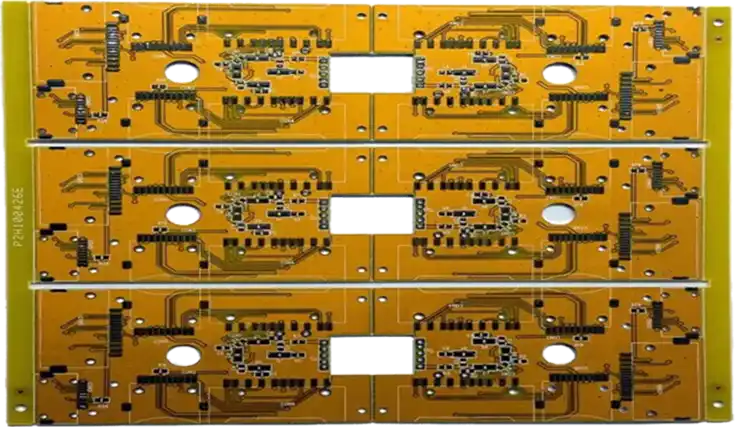
This guide explores the principles of high-speed PCB design, the manufacturing and assembly considerations involved, the major applications, common design challenges, and how Kingda supports high-speed PCB and PCBA projects from prototype to production.
What Are High-Speed PCBs?
A High-Speed PCB is a printed circuit board designed to maintain reliable signal transmission when transmission-line effects become significant.
There is no universal frequency threshold that automatically defines a PCB as “high speed.” A frequently cited number such as 50 MHz can be misleading because the need for high-speed design techniques depends heavily on signal rise time, edge rate, interconnect length, propagation delay, interface technology, and operating frequency.
A relatively low-frequency digital signal with a very fast edge can still require transmission-line analysis, while a higher-frequency signal with a slower edge may behave differently.
Typical high-speed PCB applications include:
- High-speed memory interfaces
- PCIe systems
- USB interfaces
- Ethernet
- SerDes
- High-speed ADC/DAC circuits
- Data-center equipment
- AI computing systems
- Telecom equipment
- Automotive Ethernet
- 5G infrastructure
- High-speed industrial communication
The objective of high-speed PCB design is to ensure that the signal reaches its destination with acceptable levels of distortion, loss, noise, and timing variation.
Key Features of High-Speed PCB Design
A successful high-speed PCB design requires careful planning from the schematic and stack-up stages through routing, simulation, fabrication, and assembly.
Signal Integrity
Signal integrity (SI) is one of the most important considerations in high-speed electronics.
As digital edge rates increase, traces behave as transmission lines rather than simple conductive connections. Improper routing can result in:
- Reflections
- Ringing
- Overshoot and undershoot
- Crosstalk
- Insertion loss
- Timing variation
- Signal attenuation
The goal is to ensure that the electrical waveform arriving at the receiver remains within the required voltage and timing margins.
Designers can improve signal integrity by:
- Controlling trace impedance
- Maintaining appropriate reference planes
- Minimizing unnecessary vias
- Reducing stubs
- Optimizing differential pairs
- Keeping high-speed paths short where practical
- Managing connectors and transition structures
Impedance Control
Controlled impedance is essential for many high-speed interfaces.
Characteristic impedance is determined by factors such as:
- Trace width
- Copper thickness
- Dielectric thickness
- Dielectric constant
- Distance to the reference plane
- Trace geometry
- PCB stack-up
Common target values may include 50 ohms for single-ended routing and 90 or 100 ohms for certain differential interfaces, but the correct value must always be determined by the specific interface specification.
Impedance should be designed into the PCB stack-up before routing rather than treated as a final manufacturing adjustment.
Kingda provides controlled-impedance PCB manufacturing and engineering support, with published capabilities covering high-speed, high-frequency, HDI, multilayer, flexible, rigid-flex, and other advanced PCB technologies. (Kingda)
Return Paths
A high-speed signal always has a return-current path.
A continuous reference plane directly adjacent to the signal layer can provide a low-impedance return path and help reduce loop area.
Problems can occur when a high-speed trace crosses:
- Plane splits
- Voids
- Gaps
- Reference-plane transitions
- Poorly designed layer changes
Designers should therefore consider signal and return paths together rather than routing the signal alone.
Differential Signaling
Differential signaling uses two complementary conductors to transmit information.
It is widely used in high-speed interfaces because differential signaling can provide improved immunity to common-mode noise when the pair is routed and terminated correctly.
Important design considerations include:
- Pair spacing
- Differential impedance
- Length matching where required
- Symmetrical geometry
- Continuous reference planes
- Via-transition consistency
Crosstalk
Crosstalk occurs when electromagnetic energy from one trace couples into another.
It becomes more significant when:
- Signal edges are fast
- Adjacent traces are closely spaced
- Parallel routing is long
- Return paths are poorly controlled
Common mitigation techniques include:
- Increasing trace spacing
- Reducing parallel routing length
- Using appropriate reference planes
- Separating sensitive and noisy signals
- Optimizing stack-up
- Controlling differential-pair geometry
Electromagnetic Interference
EMI can become a significant issue in high-speed PCB designs because fast voltage and current transitions can generate unwanted electromagnetic energy.
Kingda’s engineering guidance identifies high-speed switching, poor grounding, large loop areas, impedance mismatch, and inadequate shielding among the causes that can contribute to PCB EMI problems. (Kingda)
Good EMI control practices include:
- Continuous ground planes
- Short return paths
- Small current-loop areas
- Proper power decoupling
- Appropriate circuit partitioning
- Controlled impedance
- Shielding when required
Power Integrity
A high-speed processor, FPGA, memory device, or networking ASIC can generate rapidly changing current demand.
The power distribution network (PDN) must therefore maintain stable supply voltage during transient conditions.
Power integrity (PI) design involves:
- Power planes
- Ground planes
- Decoupling capacitors
- Via inductance
- Plane impedance
- Voltage drop
- Current return paths
- Transient response
For advanced designs, SI and PI analysis should be performed together because the power and signal networks influence each other.
Thermal Management
High-speed systems often combine high-performance processors with high switching activity and high power density.
Thermal problems can affect:
- Component lifetime
- Signal stability
- Solder-joint reliability
- Electrical performance
- System stability
Thermal solutions may include:
- Large copper areas
- Thermal vias
- Copper planes
- Heat sinks
- Metal-core structures
- Thermal interface materials
- Airflow
- System-level liquid cooling where necessary
High-Speed PCB Stack-Up Design
The PCB stack-up forms the foundation of high-speed electrical performance.
A well-designed multilayer stack-up typically places high-speed signal layers close to continuous reference planes.
A simplified example might be:
Signal / Ground / Signal / Power / Ground / Signal
However, the correct stack-up depends on the PCB’s interface requirements, number of layers, board thickness, material properties, current requirements, and manufacturability.
Dielectric Thickness
The distance between a signal trace and its reference plane strongly affects impedance.
Even a relatively small change in dielectric thickness can change characteristic impedance.
Dielectric Constant and Loss Tangent
The laminate’s electrical properties influence:
- Propagation speed
- Characteristic impedance
- Insertion loss
- Dispersion
For very high-speed or high-frequency applications, advanced low-loss laminates may be required.
Copper Thickness and Roughness
Copper thickness influences impedance and current carrying capability.
At higher frequencies, conductor surface roughness can also contribute to transmission loss, so material and copper-foil selection should be part of the high-speed design process.
High-Speed PCB Manufacturing Considerations
High-speed PCB manufacturing requires tighter coordination between electrical design and fabrication.
1. Stack-Up Development
The manufacturing partner should confirm:
- Layer count
- Dielectric thickness
- Copper thickness
- Laminate type
- Impedance targets
- Signal/reference layer relationships
The final stack-up should be approved before production.
2. Precision Imaging and Etching
Trace width and spacing directly influence impedance.
Etching variation can therefore affect electrical performance, especially on fine-line and controlled-impedance boards.
3. Drilling and Via Formation
High-speed boards may require advanced via technologies such as:
- Blind vias
- Buried vias
- Microvias
- Back-drilled vias
- Via-in-pad
The appropriate technology depends on the signal speed, board architecture, component pitch, and manufacturing capability.
4. Multilayer Lamination
Layer registration and dielectric consistency are important to maintaining a predictable stack-up.
Poor registration or uncontrolled dielectric thickness can result in impedance variation.
5. Copper Plating
Copper plating affects both electrical performance and reliability.
The manufacturer must maintain appropriate control over:
- Plating thickness
- Uniformity
- Hole-wall quality
- Surface condition
6. Surface Finish
Common surface finishes include:
- ENIG
- ENEPIG
- OSP
- Immersion tin
- Immersion silver
- Lead-free HASL
For high-speed applications, finish selection should be considered together with component package, assembly process, reliability requirements, and electrical performance.
High-Speed PCB Assembly
The quality of high-speed PCB assembly can directly affect final electrical performance.
Even when the PCB fabrication is excellent, problems with component placement, soldering, connectors, or assembly defects can compromise the system.
Component Placement
High-speed components should be positioned according to the signal-flow architecture.
For critical interfaces, designers should minimize:
- Trace length
- Unnecessary vias
- Excessive layer transitions
- Large routing loops
Components should also be placed with power-delivery and thermal requirements in mind.
Soldering
SMT assembly typically uses solder paste printing, automated placement, and controlled reflow soldering.
For advanced packages such as BGA and QFN, proper stencil design and reflow control are especially important.
Inspection
A high-speed PCBA may require:
- SPI
- AOI
- X-ray inspection
- ICT
- Functional testing
Kingda’s published quality-control flow is:
IQC → SPI → SMT/THT Assembly → AOI → X-Ray → ICT/FCT → OQC
The company also lists 3D SPI, AOI, X-ray, FAI, ICT, and FCT capabilities. (Kingda)
Testing
Depending on application requirements, high-speed PCB testing may include:
- Continuity
- Insulation
- Controlled impedance
- Functional verification
- High-speed interface testing
- Signal-integrity validation
- EMC/EMI testing
For high-speed prototypes, testing requirements should be established before manufacturing begins so the appropriate fixtures and test points can be incorporated into the design.
Role of High-Speed PCBs in Advanced Electronics
The demand for high-speed electronics continues to increase as data volumes grow.
5G Infrastructure
5G systems require high data throughput and increasingly sophisticated RF and digital processing hardware.
High-Speed PCBs support networking, communication processing, switching, and high-frequency signal transmission.
Artificial Intelligence and High-Performance Computing
AI servers and high-performance computing systems depend on fast communication between processors, memory, accelerators, and network interfaces.
These systems increasingly require:
- High-speed backplanes
- High-speed memory
- High-bandwidth interconnects
- Advanced power delivery
- Advanced thermal management
Data Centers
Modern data centers rely on high-speed networking and storage systems to transfer large amounts of information with low latency.
PCB performance is critical in:
- Network switches
- Routers
- Server motherboards
- Storage systems
- Accelerator cards
- Backplanes
Automotive Electronics
Modern vehicles increasingly use high-speed links for:
- ADAS
- Automotive Ethernet
- Cameras
- Radar
- Infotainment
- Domain controllers
- Vehicle networking
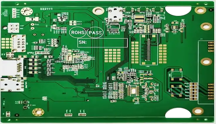
Automotive high-speed PCBs must combine electrical performance with mechanical and environmental reliability.
Aerospace and Defense
High-speed circuits are used in:
- Avionics
- Radar
- Communications
- Navigation
- Satellite systems
- Control electronics
These applications may require additional environmental testing and reliability controls.
Consumer Electronics
High-speed PCBs are increasingly used in:
- Smartphones
- Tablets
- Laptops
- Wearables
- Gaming systems
- Routers
- Cameras
Medical Electronics
Medical imaging and diagnostic systems can require high-speed data transfer for sensors and image-processing systems.
Applications include:
- MRI
- CT
- Ultrasound
- Patient monitoring
- Medical imaging interfaces
Industrial Automation and Robotics
Industrial equipment uses high-speed communication for:
- Industrial Ethernet
- Machine vision
- Motion control
- Sensors
- Data acquisition
- Robotics
Advanced High-Speed PCB Design Using ECAD and Simulation
Designing a complex high-speed PCB manually without simulation and automated constraints can introduce unnecessary risk.
Modern ECAD tools can support:
- Stack-up planning
- Impedance calculation
- Length matching
- Differential-pair routing
- Design-rule checking
- SI simulation
- PI analysis
- Thermal analysis
- 3D mechanical verification
Simulation can identify potential issues before PCB fabrication.
For demanding designs, engineers may evaluate:
- Eye diagrams
- Insertion loss
- Return loss
- Crosstalk
- Propagation delay
- Skew
- PDN impedance
The objective is to identify and resolve electrical problems while the design is still editable.
High-Speed PCB Design Best Practices
Keep High-Speed Interconnects Short
Shorter interconnects generally reduce propagation delay and loss.
Maintain Continuous Reference Planes
Avoid routing critical high-speed traces across gaps in the reference plane.
Control Differential-Pair Geometry
Maintain consistent pair spacing and impedance throughout the route.
Minimize Vias and Stubs
Unnecessary vias can introduce discontinuities.
For especially demanding interfaces, back drilling or optimized via structures may be considered.
Separate Noisy and Sensitive Circuits
High-speed digital switching circuits should be appropriately separated from sensitive analog, RF, or sensor circuitry.
Optimize Power Delivery
Place decoupling capacitors close to device power pins and minimize the associated current-loop area.
Simulate Before Fabrication
Use SI/PI simulation to validate critical interfaces before manufacturing.
Future Trends in High-Speed PCB Technology
Advanced Low-Loss Materials
As data rates increase, low-loss dielectric materials will become increasingly important.
Advanced material systems based on technologies such as PTFE, LCP, and other low-loss constructions may be used for demanding high-frequency and high-speed applications.
AI-Assisted PCB Design
AI-assisted EDA tools are increasingly being used for:
- Routing optimization
- Constraint management
- SI analysis
- DFM
- Stack-up optimization
- Component placement
These tools can help engineers reduce repetitive work while retaining human engineering control.
Higher Data Rates
The continued development of AI computing, cloud infrastructure, networking, and high-speed memory will drive demand for PCBs capable of handling increasingly high-speed interfaces.
More Advanced HDI
Miniaturization will continue to drive:
- Microvias
- Fine-line circuits
- Any-layer HDI
- Via-in-pad
- Advanced multilayer stack-ups
Integration of Electrical and Thermal Design
As power density rises, signal integrity and thermal management will increasingly need to be solved together rather than independently.
How Kingda Supports High-Speed PCB Projects
For customers developing high-speed electronic products, choosing a supplier with both high-speed PCB manufacturing and PCBA capabilities can simplify development and production.
Kingda is a one-stop PCB and PCBA manufacturer founded in 2013. Its published capabilities include high-speed PCB, high-frequency PCB, HDI PCB, flexible PCB, rigid-flex PCB, multilayer PCB, controlled-impedance PCB, PCB assembly, component sourcing, testing, and finished-product assembly. (Kingda)
High-Speed and High-Frequency PCB Manufacturing
Kingda lists high-speed and high-frequency PCB manufacturing among its technical capabilities and provides PCB solutions for communication, AI, industrial, automotive, medical, and other applications. (Kingda)
Controlled-Impedance Engineering
For high-speed designs, impedance control should be integrated into the PCB stack-up and fabrication process from the beginning.
Kingda provides engineering support for PCB design, DFM/DFA, stack-up review, manufacturing optimization, and controlled-impedance requirements. (Kingda)
Advanced SMT Assembly
High-speed PCBs frequently use complex component packages.
Kingda states that its SMT capabilities support fine-pitch components, including 0.35 mm-pitch BGA and 01005 passive components, together with X-ray inspection and other assembly controls. (Kingda)
Comprehensive Inspection and Testing
Kingda’s quality-control process integrates:
IQC → SPI → SMT/THT Assembly → AOI → X-Ray → ICT/FCT → OQC
This provides inspection and testing throughout the production cycle rather than relying only on final inspection. (Kingda)
DFM and DFA Support
Kingda provides DFM/DFA engineering services, Gerber review, BOM verification, pick-and-place file verification, component sourcing support, and manufacturing optimization. (Kingda)
For a high-speed PCB, early engineering review is especially valuable because problems with impedance, stack-up, component placement, and routing are much less expensive to fix before fabrication.
Component Procurement
Kingda integrates component procurement into its one-stop PCBA service and states that it maintains supplier relationships with major distributors to support component availability and delivery. (Kingda)
Quality Management and Traceability
Kingda reports IATF 16949:2016, ISO 13485:2016, and ISO 9001:2015 certifications, with additional certifications and qualifications including ISO 14001 and UL listed on its website. (Kingda)
Its published quality process also emphasizes production traceability from incoming materials through final shipment. (Kingda)
Prototype to Volume Production
Kingda supports rapid PCBA prototyping, low-volume manufacturing, and high-volume production, allowing customers to move from engineering prototypes toward production using an integrated manufacturing partner. (Kingda)
High-Speed PCB Design and Manufacturing Checklist
Before sending a high-speed PCB into production, engineers should verify:
Design
- Signal integrity requirements
- Controlled impedance
- Differential-pair requirements
- Length matching
- Return paths
- Reference planes
- Via structures
- Crosstalk
- Thermal requirements
Manufacturing
- Approved PCB stack-up
- Correct laminate
- Dielectric thickness
- Copper thickness
- Impedance tolerance
- Layer registration
- Surface finish
- Via fabrication requirements
Assembly
- Component placement
- BGA/QFN requirements
- Stencil design
- Reflow profile
- AOI
- X-ray
- ICT/FCT
- Functional testing
Engineering
- DFM review
- DFA review
- SI simulation
- PI analysis
- Thermal analysis
- Prototype validation
This approach helps reduce the risk of discovering critical electrical or manufacturing problems after production begins.
Conclusion
High-Speed PCB design and manufacturing are becoming increasingly important as AI, 5G, cloud computing, high-performance computing, automotive electronics, medical systems, and industrial automation demand faster and more reliable data transmission.
The challenge is not simply making a PCB capable of carrying a faster signal. Successful high-speed PCB development requires coordinated control of signal integrity, impedance, return paths, crosstalk, power integrity, EMI, thermal performance, materials, stack-up, fabrication tolerances, and assembly quality.
The complete process can be summarized as:
System Requirements → Stack-Up Design → SI/PI Analysis → Controlled Routing → DFM/DFA → Precision PCB Fabrication → SMT/THT Assembly → Inspection → Electrical/Functional Testing
For companies looking for a reliable High-Speed PCB manufacturer and PCBA partner, Kingda combines high-speed and high-frequency PCB manufacturing, controlled-impedance solutions, HDI, SMT/THT assembly, component sourcing, DFM/DFA engineering, inspection, testing, and scalable production. (Kingda)
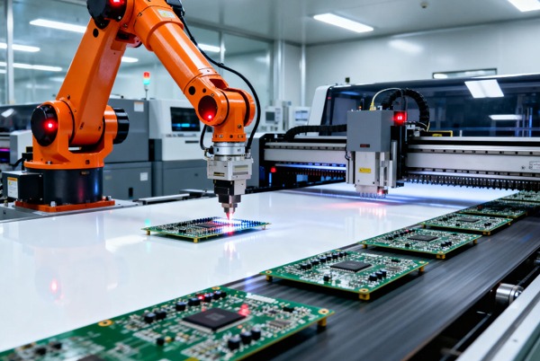
With an integrated manufacturing model, Kingda can support customers from high-speed PCB prototypes and engineering validation to low-volume and production-scale manufacturing, helping turn complex high-speed designs into reliable electronic products.