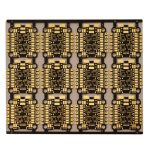
Radar PCB Manufacturer for High-Frequency Applications
Modern radar systems require printed circuit boards capable of handling high-frequency signals with excellent electrical stability, controlled impedance and reliable signal integrity. From automotive radar and industrial sensing to aerospace, defense and weather monitoring, the PCB is a critical part of the radar signal chain.
As a professional Radar PCB Manufacturer, we provide advanced PCB fabrication solutions for demanding RF and microwave applications. Our capabilities include high-frequency materials, multilayer structures, controlled-impedance construction, fine-line routing and specialized via technologies.
Our Radar PCB solutions can be manufactured using FR-4, high-TG FR-4, PTFE, Teflon-based materials, Rogers, Taconic, Arlon, Isola, Panasonic and other high-performance laminates according to electrical and mechanical requirements.
For projects requiring advanced RF performance, our High Frequency PCB Manufacturing capabilities support specialized material selection, multilayer stackups and impedance-controlled structures.
What Is a Radar PCB?
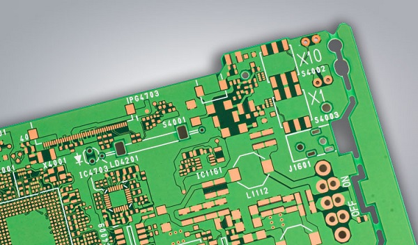
A radar PCB is a printed circuit board specifically designed to support radar systems that transmit, receive and process electromagnetic or radio-frequency signals.
Unlike conventional low-frequency circuit boards, radar boards must maintain predictable electrical characteristics at high frequencies. Small variations in dielectric thickness, trace geometry, copper surface, via structure or impedance can affect signal transmission and overall system performance.
A typical radar PCB may integrate RF transmission circuits, receiver circuits, antenna interfaces, signal-processing electronics, power-management circuits and control electronics.
Depending on the application, the board may require:
- High-frequency or low-loss laminate materials
- Controlled impedance
- RF and microwave routing
- Low dielectric-loss materials
- Precise multilayer stackups
- Blind and buried vias
- Fine-line and fine-spacing technology
- High-quality surface finishes
- Strict manufacturing tolerances
For compact radar systems, an advanced HDI PCB structure can also improve routing density and reduce interconnection length.
How Does a Radar PCB Work?
Radar systems transmit electromagnetic energy toward a target and receive the reflected signal. The radar electronics then analyze the returned signal to determine information such as distance, direction, movement and, depending on the system, other characteristics of the target.
The PCB supports several important stages of this process.
RF Signal Transmission
The transmitter generates a high-frequency signal that is routed through the PCB toward the antenna or RF front end. The transmission path must maintain controlled impedance and minimize insertion loss.
Signal Reception
The receiver captures reflected electromagnetic energy and transfers the signal to sensitive RF circuits. Because received signals can be relatively weak, the PCB must minimize unwanted noise, coupling and electromagnetic interference.
Signal Processing
After reception, the signal is processed by analog and digital circuits. Depending on the radar architecture, this may include amplification, filtering, frequency conversion, analog-to-digital conversion and digital signal processing.
Antenna Interface
The PCB provides the electrical connection between RF circuitry and the antenna system. The transition between the transmission line and antenna must be carefully designed to preserve signal integrity.
Key Features of Radar PCB Manufacturing
A reliable Radar PCB Manufacturer must control both material properties and fabrication parameters. Radar applications often operate at frequencies where conventional PCB manufacturing variations can significantly affect electrical performance.
High-Frequency Materials
Material selection is one of the most important factors in radar PCB fabrication.
Depending on operating frequency and performance requirements, suitable materials may include:
- Rogers RO4350 and related RF laminates
- Rogers RO3003
- Taconic RF materials
- PTFE-based laminates
- Low-loss high-frequency materials
- High-performance FR-4
- Hybrid RF and FR-4 constructions
The appropriate material should be selected according to dielectric constant, dissipation factor, thermal performance, mechanical requirements and cost.
Controlled Impedance
RF transmission lines must maintain a predictable characteristic impedance. A mismatch can increase signal reflection and insertion loss, reducing the efficiency of the radar signal path.
Typical impedance requirements may include 50-ohm single-ended RF transmission lines, although the actual target depends on the circuit architecture.
A professional PCB fabrication process should therefore consider trace width, copper thickness, dielectric thickness, dielectric constant and stackup geometry together.
Low-Loss Signal Transmission
High-frequency signals are more sensitive to dielectric and conductor losses. Low-loss materials can help reduce attenuation and preserve signal quality over critical transmission paths.
Precision Multilayer Construction
Radar electronics may combine RF, analog, digital and power circuits on the same PCB. A carefully engineered multilayer stackup can separate functional circuits while providing stable reference planes and controlled signal paths.
Our PCB Capabilities include multilayer construction, HDI, RF materials, controlled impedance, blind and buried vias and other advanced PCB technologies.
Fine-Line Routing
Compact radar modules often require high routing density. Fine-line PCB technology enables more RF, control and processing circuitry to be integrated into a limited board area.
Common Types of Radar PCBs
Different radar architectures require different PCB structures and electrical characteristics.
Pulse Radar PCB
Pulse radar transmits electromagnetic energy in pulses and analyzes the returned signals. The PCB must support accurate high-frequency transmission and reception while maintaining timing and signal integrity.
Doppler Radar PCB
Doppler radar measures changes in the frequency of reflected signals to determine relative movement. These systems require stable RF transmission and sensitive receiver circuitry.
Weather Radar PCB
Weather radar systems use electromagnetic signals to detect precipitation and atmospheric conditions. Their PCB assemblies must support reliable high-frequency operation and long-term environmental stability.
Passive Radar PCB
Passive radar systems use existing electromagnetic signals rather than relying exclusively on their own high-power transmitter. Their receiver and signal-processing circuits require careful RF design and low-noise PCB construction.
Automotive Radar PCB
Automotive radar is widely used for vehicle detection, distance measurement and advanced driver-assistance functions. Compact dimensions, high-frequency operation, thermal stability and reliable manufacturing are particularly important.
Radar PCB Applications
Radar PCB technology is used across multiple industries where reliable electromagnetic sensing and target detection are required.
Automotive Radar
Automotive radar systems can support functions such as adaptive cruise control, blind-spot detection, collision warning and other ADAS technologies.
Aerospace and Defense
Radar systems are used for surveillance, navigation, tracking and target detection. These applications can require specialized high-frequency materials, multilayer structures and stringent reliability requirements.
Weather Monitoring
Meteorological radar systems use electromagnetic signals to detect precipitation and analyze atmospheric conditions.
Industrial Sensing
Industrial radar sensors can be used for distance measurement, level detection, motion sensing and process monitoring.
Security and Surveillance
Radar sensors can detect movement and position without relying exclusively on optical imaging. They can therefore be used in perimeter monitoring, access control and other security systems.
Space and Satellite Systems
Space-based radar equipment requires PCB structures capable of maintaining stable electrical and mechanical performance under demanding environmental conditions.
Radar PCB Design Considerations
Successful radar PCB development starts with the electrical requirements of the complete radar system.
1. Define the Operating Frequency
The first step is to determine the radar operating frequency and bandwidth. Material selection, trace geometry, stackup construction and impedance calculations should all be based on the actual frequency range.
2. Select the Correct Laminate
The dielectric constant and dissipation factor of the laminate influence transmission-line behavior and signal loss.
For demanding RF applications, high-frequency materials such as Rogers or Taconic may be more appropriate than conventional FR-4.
3. Develop the PCB Stackup
The stackup should define:
- Signal layers
- Ground planes
- Power planes
- Dielectric thickness
- Copper thickness
- Core and prepreg materials
- Controlled-impedance structures
- RF transmission-line geometry
The stackup should be finalized before detailed routing begins.
4. Control RF Routing
RF traces should be kept as short and direct as practical. Unnecessary bends, vias and discontinuities should be minimized.
Critical RF traces should maintain consistent geometry and an uninterrupted reference plane.
5. Manage Grounding
A stable ground structure is essential for radar PCB performance. Ground planes should be carefully designed to reduce unwanted coupling and provide appropriate return-current paths.
6. Control EMI and Crosstalk
Radar circuits can be highly sensitive to electromagnetic interference. RF, digital and power sections should be strategically arranged to minimize unwanted coupling.
Where appropriate, designers may use shielding structures, ground stitching vias and physical separation between sensitive circuits.
For complex projects, professional PCB Design & Layout Services can help evaluate stackup, impedance, EMI/EMC and manufacturability requirements before fabrication.
Radar PCB Manufacturing Process
A controlled manufacturing process is essential for maintaining the electrical characteristics required by radar applications.
Engineering Review
The manufacturing process begins with Gerber files, stackup information, material specifications and other technical documentation.
Engineering teams review the design for manufacturability, impedance requirements, material compatibility and potential production risks.
Material Preparation
The selected laminate system is prepared according to the approved stackup. RF materials must be handled carefully to maintain the specified dielectric structure.
Inner-Layer Fabrication
Inner copper layers are imaged and etched according to the circuit design. Precise registration is especially important for multilayer RF boards.
Lamination
The individual layers are laminated under controlled temperature and pressure conditions to create the required multilayer structure.
Drilling and Via Formation
Mechanical or laser drilling is used according to the PCB construction. Advanced boards may incorporate blind vias, buried vias or microvias.
Copper Plating
Through-holes and other conductive structures are plated to establish reliable electrical connections between layers.
Outer-Layer Processing
Outer copper patterns are formed and processed according to the approved design.
Surface Finishing
Depending on the application, surface finishes such as ENIG, HASL, OSP, immersion silver or ENEPIG may be selected.
Electrical Testing and Inspection
Quality control may include AOI, X-ray inspection, dimensional inspection and 100% electrical testing. These processes help verify circuit integrity and manufacturing consistency.
Why Choose a Professional Radar PCB Manufacturer?
Radar PCB fabrication requires more than conventional PCB production. The manufacturer must understand the relationship between material properties, stackup construction, impedance, RF routing and manufacturing tolerances.
A capable manufacturing partner can provide:
- High-frequency PCB fabrication
- RF and microwave PCB manufacturing
- Rogers and other specialized laminates
- Controlled-impedance PCB production
- Multilayer PCB fabrication
- HDI and microvia technology
- DFM engineering review
- Prototype and production support
- Electrical testing and inspection
- PCB assembly integration
Our PCB Manufacturing Services support advanced PCB structures from prototype development through production, including high-frequency, high-speed, HDI, multilayer, rigid-flex and controlled-impedance technologies.
Radar PCB Prototype and Production
Radar projects often require multiple development iterations before reaching volume production. A flexible manufacturing partner should therefore be capable of supporting both prototypes and production quantities.
During the prototype stage, engineers can validate:
- RF performance
- Impedance
- Antenna interface
- Signal integrity
- Thermal performance
- Mechanical fit
- Manufacturing feasibility
After validation, the same design can move into low-volume or mass production with controlled process parameters.
For customers requiring integrated electronics production, PCB Assembly Services can combine PCB fabrication with component sourcing, SMT, THT/DIP assembly, inspection and testing.
For smaller production runs and engineering validation, Low Volume PCB Assembly provides a practical solution for prototype and low-volume radar electronics.
Common Radar PCB Manufacturing Challenges
Signal Loss
Poor material selection or unsuitable transmission-line geometry can increase insertion loss at high frequencies.
Impedance Variation
Changes in trace width, dielectric thickness or material properties can affect impedance and create signal reflections.
Electromagnetic Interference
Poor layout separation or inadequate grounding can increase unwanted coupling between RF, digital and power circuits.
Thermal Stress
High-power RF components may generate substantial heat. The PCB design must provide appropriate thermal paths and material selection.
Manufacturing Tolerance
High-frequency PCB structures can be sensitive to relatively small dimensional variations. Manufacturing capability should therefore be considered during the design stage.
Material Compatibility
Hybrid constructions combining different PCB materials require careful consideration of thermal expansion, lamination conditions and mechanical reliability.
How to Select the Right Radar PCB Manufacturer
When selecting a supplier, consider more than PCB price.
Evaluate the manufacturer’s:
- High-frequency PCB experience
- RF and microwave material availability
- Controlled-impedance capability
- Multilayer and HDI manufacturing technology
- Engineering and DFM support
- Quality inspection and testing systems
- Prototype-to-production capability
- PCB assembly integration
- Material traceability and process control
- Ability to meet your required delivery schedule
The right supplier should be able to review your complete technical requirements and recommend a manufacturable PCB structure rather than simply fabricate the supplied files.
Radar PCB Manufacturing FAQs
What is a radar PCB?
A radar PCB is a printed circuit board designed to transmit, receive and process high-frequency electromagnetic signals used by radar systems.
What materials are commonly used for radar PCBs?
Common materials include high-performance FR-4, Rogers, Taconic, PTFE-based laminates and other low-loss RF materials. Material selection depends on frequency, dielectric properties, thermal requirements and mechanical design.
Why is controlled impedance important for radar PCBs?
Controlled impedance helps maintain predictable signal transmission and reduce reflections, insertion loss and signal-integrity problems in RF transmission paths.
Can radar PCBs use multilayer construction?
Yes. Multilayer construction is widely used to integrate RF, analog, digital and power circuits while providing dedicated signal and ground layers.
Are Rogers materials suitable for radar PCBs?
Rogers materials are commonly used in demanding RF and microwave applications because their electrical properties can provide stable high-frequency performance.
Can radar PCBs use HDI technology?
Yes. HDI can be useful for compact radar modules that require high routing density, fine-pitch components and reduced interconnection length. The appropriate HDI structure should be selected according to electrical and manufacturing requirements.
Can you manufacture and assemble radar PCBAs?
Yes. PCB fabrication can be combined with component procurement, SMT, through-hole assembly, inspection and testing to provide an integrated manufacturing solution.
Conclusion
A radar system depends heavily on the electrical performance and reliability of its PCB. From material selection and controlled impedance to RF routing, multilayer stackup, grounding and manufacturing precision, every part of the PCB process can influence radar performance.
Choosing an experienced Radar PCB Manufacturer helps ensure that the board is designed and manufactured around the actual frequency, signal-integrity, thermal and mechanical requirements of the application.
With advanced High Frequency PCB, RF PCB, Microwave PCB and multilayer manufacturing capabilities, Gopcba provides PCB solutions for automotive radar, industrial sensing, aerospace, defense, weather monitoring, security and other high-frequency applications.
Contact Gopcba to discuss your radar PCB requirements and obtain a manufacturing solution tailored to your design, material and production requirements.