Automotive Sensor PCB Manufacturing: Materials, Processes & Quality Control
Automotive sensors act as critical sensing components within modern vehicles. They continuously collect information related to temperature, pressure, position, speed, acceleration, environmental conditions, and vehicle operating status. Their performance directly affects powertrain control, driver assistance, safety systems, and vehicle intelligence.
At the center of these sensing systems is the Automotive Sensor PCB, which provides electrical connections, signal transmission, power distribution, and mechanical support for electronic components.
Unlike conventional consumer-electronics circuit boards, automotive sensor PCBs must operate reliably under demanding conditions, including temperature fluctuations, vibration, mechanical shock, humidity, electromagnetic interference, and long operating cycles. As a result, Automotive PCB Manufacturing requires careful control of materials, fabrication processes, dimensional accuracy, electrical performance, and reliability.
Material selection is the foundation of reliable automotive PCB manufacturing. The laminate, copper foil, solder mask, surface finish, and other materials must be selected according to the sensor’s operating environment and electrical requirements.
Standard FR-4 may be suitable for many automotive control applications, while high-Tg FR-4 and specialized high-performance laminates may be required for applications involving elevated temperatures, repeated thermal cycling, or demanding reliability requirements.
For automotive electronics, high-Tg materials can provide improved dimensional stability and resistance to thermal stress. Specialized materials may also be required for high-frequency radar, communication, or other RF applications.
GOPCBA’s PCB Substrate Material Selection Guide provides additional information about FR-4, high-Tg materials, Rogers, PTFE, polyimide, and other PCB substrate technologies.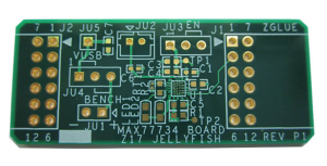
Copper foil is another important material. Its thickness must be selected according to current-carrying requirements, signal characteristics, thermal conditions, and mechanical constraints. For power-related sensor electronics, thicker copper may be considered to improve current capacity and thermal performance.
The solder mask must also provide strong adhesion, insulation, chemical resistance, and environmental durability. These characteristics help protect copper circuits from moisture, contamination, corrosion, and accidental electrical contact.
Automotive sensor PCB materials should generally provide:
- High thermal stability
- Good dimensional stability
- Strong copper adhesion
- Low moisture absorption
- Reliable electrical insulation
- Good chemical resistance
- Long-term environmental durability
- Consistent manufacturing performance
Material certification and incoming inspection are also important parts of the manufacturing process. Each material batch should be checked against approved specifications before entering production.
Manufacturing an automotive sensor PCB involves multiple interconnected processes. Each stage must be controlled because dimensional or material variation introduced during one operation can affect subsequent processes.
A typical manufacturing workflow includes material preparation, inner-layer fabrication, lamination, drilling, copper plating, outer-layer circuit formation, solder mask application, surface finishing, final forming, inspection, and electrical testing.
The manufacturing process begins by preparing laminates, copper foils, prepreg, and other materials according to the approved PCB stack-up.
Large production panels are cut into the required dimensions using precision equipment. Dimensional accuracy is important because panel dimensions influence subsequent imaging, lamination, drilling, and registration processes.
The material should also be stored under controlled environmental conditions to minimize moisture absorption and dimensional changes.
For multilayer automotive sensor PCBs, inner-layer circuits are created before lamination.
The copper surface is cleaned and prepared before the circuit pattern is transferred through imaging. After exposure and development, the required copper pattern is formed through etching and other controlled processes.
Automated optical inspection can then be used to identify defects such as:
- Open circuits
- Short circuits
- Missing copper
- Excess copper
- Trace-width deviations
- Pattern defects
Accurate inner-layer fabrication is particularly important for complex automotive boards because dimensional errors can accumulate during subsequent lamination and registration processes.
For an Automotive Multilayer PCB, individual cores, copper layers, and prepreg materials must be precisely aligned and laminated into a single structure.
Temperature, pressure, heating rate, cooling rate, resin flow, and layer registration must be carefully controlled.
Poor lamination can cause:
- Layer misalignment
- Delamination
- Internal voids
- Resin starvation
- Board warpage
- Unstable dielectric thickness
For high-reliability automotive applications, stable lamination is especially important because changes in dielectric thickness or layer position can affect both mechanical reliability and electrical performance.
GOPCBA’s Automotive Multilayer PCB Manufacturing capabilities address multilayer construction, thermal management, high-density interconnections, impedance control, and automotive reliability requirements.
After lamination, holes are drilled according to the PCB design.
Mechanical CNC drilling is commonly used for conventional through holes and vias, while laser drilling may be used for microvias and advanced HDI structures.
The drilling process must control:
- Hole diameter
- Hole position
- Drill depth
- Hole-wall quality
- Registration accuracy
- Burr formation
- Resin residue
After drilling, the hole walls undergo desmear and metallization processes. Electroless copper and subsequent electroplating create conductive copper layers inside the holes, allowing different PCB layers to communicate electrically.
For high-density automotive electronics, advanced via technologies can provide additional routing flexibility.
As automotive sensors become smaller while integrating more functions, conventional through-hole structures may not provide sufficient routing density.
HDI PCB technology uses fine traces, microvias, blind vias, buried vias, and sequential buildup structures to increase interconnection density within a smaller board area.
These technologies are particularly useful for compact sensor modules, ADAS electronics, radar systems, cameras, communication modules, and other highly integrated automotive applications.
GOPCBA’s HDI PCB Design and Manufacturing Guide explains important considerations involving microvias, blind and buried vias, stack-up design, routing density, signal integrity, and manufacturability.
Circuit fabrication is one of the most important stages in automotive PCB production.
The required circuit image is transferred to the copper surface using a controlled imaging process. After development, unwanted copper is removed through etching, leaving the required conductive pattern.
Trace width and spacing must remain within the specified tolerances.
This is particularly important for sensor circuits because signal accuracy can be affected by changes in trace geometry, copper thickness, impedance, and electrical isolation.
For high-speed automotive systems, including radar, cameras, communication interfaces, and advanced driver assistance electronics, PCB layout and manufacturing must also consider signal integrity.
The relationship between trace width and copper thickness becomes especially important when the PCB combines signal circuits with power distribution.
After circuit formation, a solder mask is applied to protect the copper conductors and prevent unwanted solder bridging during assembly.
The solder mask is selectively exposed and developed so that component pads and other required conductive areas remain accessible.
A properly controlled solder mask provides:
- Electrical insulation
- Copper protection
- Improved environmental resistance
- Reduced risk of solder bridging
- Improved long-term PCB durability
Silkscreen or legend information can then be applied to identify component locations, polarity, product information, test points, and other assembly references.
For automotive applications, markings should remain clear and durable throughout assembly, testing, and service.
Surface finishing protects exposed copper and improves solderability.
Common PCB surface finishes include:
- ENIG
- ENEPIG
- Immersion silver
- Immersion tin
- HASL
The appropriate surface finish depends on component package requirements, soldering technology, environmental conditions, electrical requirements, and product lifetime.
ENIG, for example, provides a relatively flat surface and good oxidation resistance, making it suitable for fine-pitch components and various high-reliability PCB applications.
After surface finishing, the PCB is routed, punched, or otherwise formed into its final dimensions. Edge quality is inspected to ensure that there are no excessive burrs, sharp edges, cracks, or mechanical defects.
Quality control is essential because automotive electronic systems often require long service life and stable performance under harsh operating conditions.
A reliable manufacturing process should establish inspection points from incoming material inspection through final product testing.
The inspection process may include:
AOI systems inspect circuit patterns and can identify opens, shorts, missing copper, excessive copper, dimensional deviations, and other visible defects.
X-ray inspection can be used to evaluate hidden structures that cannot be completely inspected from the external surface, including internal connections and certain via or solder-joint structures.
Electrical testing verifies circuit continuity and isolation. It helps identify open circuits and short circuits before the finished PCB is released.
Board thickness, hole diameter, hole position, copper thickness, overall dimensions, and other critical mechanical characteristics should be measured against approved specifications.
Depending on the application, automotive sensor PCBs may require environmental and reliability testing involving:
- Thermal cycling
- High-temperature exposure
- Humidity testing
- Vibration testing
- Mechanical shock
- Insulation resistance
- Dielectric withstand
- Solderability
- Surface-finish reliability
These tests help verify whether the PCB can maintain stable electrical and mechanical performance during its expected service life.
Automotive electronics require strong process traceability.
A manufacturing system should be capable of connecting finished products with relevant production information, including:
- Raw-material batches
- Production dates
- Manufacturing equipment
- Process parameters
- Inspection results
- Operator information
- Testing records
- Finished-product identification
Traceability helps manufacturers investigate quality issues quickly and identify the source of potential process deviations.
For automotive supply chains, consistent production documentation and process control are particularly important because the same PCB design may be produced across multiple production batches.
Automotive electronics are developing toward smaller dimensions, greater integration, higher processing speeds, and increased functionality.
These trends are driving the adoption of advanced PCB technologies.
HDI structures allow more interconnections to be placed within a smaller board area. Microvias and sequential buildup technologies can help improve component breakout and routing density.
Automotive radar and communication systems can operate at high frequencies, creating demanding requirements for dielectric properties, copper roughness, impedance control, and dimensional accuracy.
For these applications, specialized high-frequency laminates may be required instead of conventional materials.
Automotive power electronics, battery systems, motor controllers, and related systems may require increased current-carrying capacity and improved heat dissipation.
A Heavy Copper PCB can increase copper cross-sectional area, reduce conductor resistance, improve current-carrying capacity, and support thermal management in demanding automotive power applications.
Modern vehicles increasingly use high-speed communication interfaces, radar, cameras, Ethernet, and other data-intensive systems.
For these applications, trace width, dielectric thickness, copper characteristics, reference planes, stack-up configuration, and impedance must be considered together.
Automotive sensor PCBs can be used across many vehicle systems.
Engine and Powertrain Sensors
Sensor electronics can monitor temperature, pressure, position, speed, and other parameters required for engine and powertrain control.
Battery Management Systems
Electric and hybrid vehicles rely on electronic monitoring systems to measure battery voltage, temperature, current, and other operating parameters.
ADAS and Safety Systems
Advanced driver assistance systems use cameras, radar, ultrasonic sensors, and other sensing technologies to support functions such as collision warning, adaptive cruise control, blind-spot monitoring, and automatic emergency braking.
Vehicle Body Electronics
Sensors and control modules are also used for doors, lighting, HVAC systems, seating systems, windows, and other vehicle functions.
Automotive Radar
Radar systems require highly controlled high-frequency signal transmission. PCB materials, stack-up configuration, impedance, surface characteristics, and manufacturing precision can all influence radar performance.
Automotive projects often require both bare PCB fabrication and component assembly.
Instead of treating PCB fabrication and assembly as completely separate processes, an integrated workflow can improve communication between engineering, procurement, fabrication, assembly, inspection, and testing.
GOPCBA provides One-Stop PCB Assembly Services covering PCB fabrication, component sourcing, SMT assembly, through-hole assembly, inspection, testing, and production support.
This approach can be especially useful for automotive sensor projects that require:
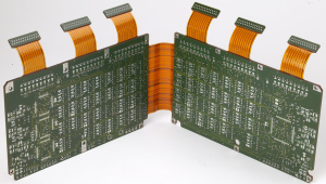
- Prototype development
- NPI production
- Low-volume manufacturing
- Component sourcing
- SMT assembly
- Electrical testing
- Functional testing
- Volume production
Early coordination between PCB fabrication and assembly can also help identify DFM and DFA issues before mass production.
Automotive electronic systems cannot be evaluated using the same standards as ordinary consumer electronics.
A vehicle may experience repeated temperature changes, continuous vibration, humidity, mechanical shock, electromagnetic interference, chemical exposure, and long operating cycles.
As a result, the High-Reliability PCB used in automotive sensors must maintain stable electrical and mechanical performance throughout its expected service life.
Achieving this reliability requires more than a single inspection step. It depends on the complete manufacturing system, including:
- Appropriate material selection
- Accurate circuit fabrication
- Stable multilayer lamination
- Reliable hole metallization
- Controlled impedance where required
- High-quality surface finishing
- Automated inspection
- Electrical testing
- Reliability testing
- Production traceability
- Consistent process control
Automotive sensor PCB manufacturing is a comprehensive engineering process involving material selection, circuit fabrication, drilling, multilayer lamination, copper plating, solder mask application, surface finishing, forming, inspection, and reliability testing.
As vehicles become increasingly intelligent, connected, electrified, and automated, automotive sensors are becoming more sophisticated. This places higher requirements on PCB density, signal integrity, thermal management, mechanical reliability, and manufacturing consistency.
From conventional sensor circuits to ADAS, automotive radar, battery management systems, power electronics, and high-speed communication modules, the right PCB technology is essential for stable electronic performance.
A combination of Automotive PCB Manufacturing, Automotive Multilayer PCB, HDI PCB, suitable materials, advanced manufacturing processes, and rigorous quality control can provide a reliable foundation for next-generation automotive electronics.
For demanding automotive projects, selecting a PCB manufacturing partner with experience in high-density, high-frequency, multilayer, high-current, and high-reliability technologies can help reduce manufacturing risks and support the transition from prototype to stable production.