Complex PCB Manufacturing: Why Advanced Processes Matter
As electronic products become smaller, faster, and more power-intensive, conventional PCB fabrication processes are often no longer sufficient. Modern industrial control systems, power electronics, medical equipment, automotive electronics, communications hardware, computing platforms, and other demanding applications increasingly require specialized structures and manufacturing techniques.
Complex PCB Manufacturing is therefore more than simply producing a circuit board with additional layers. It involves coordinating material selection, circuit geometry, copper distribution, drilling, plating, lamination, surface treatment, mechanical features, and inspection to achieve the required electrical, mechanical, and reliability performance.
For high-end electronic products, manufacturing capability can directly affect signal integrity, current-carrying capacity, thermal performance, dimensional accuracy, assembly compatibility, and long-term service reliability.
A successful complex PCB project begins with a manufacturing strategy that considers the entire design rather than treating each special process as an isolated operation.
Key Complex PCB Manufacturing Processes
Different electronic applications require different combinations of advanced manufacturing processes. Some designs may require heavy copper for high-current applications, while others may depend on resin-filled vias, castellated holes, controlled mechanical features, or specialized internal structures.
The following processes represent several important techniques used when standard PCB fabrication cannot fully satisfy a design requirement.
Heavy Copper PCB Manufacturing for High-Power Applications
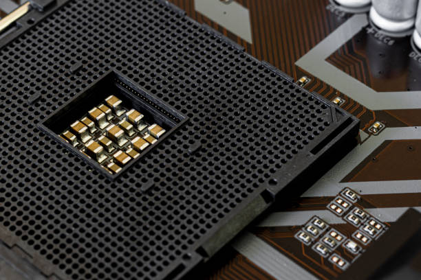
A Heavy Copper PCB is designed with significantly greater copper thickness than a conventional circuit board. It is particularly useful when the PCB must carry high current, withstand elevated thermal loads, or provide enhanced mechanical strength in copper conductors.
The main manufacturing challenges involve maintaining consistent copper thickness, controlling etching, achieving reliable plating, and managing thermal and dimensional effects during fabrication.
Increasing copper thickness changes the relationship between conductor width, spacing, etching behavior, and current capacity. If the process is not properly controlled, excessive undercutting or uneven copper distribution can affect the final geometry.
Manufacturers therefore need to optimize:
- Copper thickness and distribution
- Plating parameters
- Etching compensation
- Layer-to-layer registration
- Lamination conditions
- Thermal management
- Hole plating reliability
- Final dimensional inspection
Heavy copper construction can help reduce conductor resistance and heat generation, but material selection and overall stack-up design remain important. The copper structure must work together with the dielectric system and thermal design rather than being considered independently.
For applications involving power conversion, motor drives, industrial power supplies, battery systems, and other high-current electronics, a properly engineered High-Reliability PCB can provide a more stable platform for long-term operation.
Specialized Routing and Internal Structures
Complex PCB designs may incorporate specialized internal circuit structures that cannot be produced effectively using basic fabrication methods.
When the routing geometry becomes increasingly dense, engineers must consider not only whether a trace can physically be manufactured, but also whether its electrical characteristics, insulation spacing, thermal behavior, and mechanical reliability remain acceptable.
This is particularly important when multiple functions share a compact board area.
Precision Control of Complex Circuit Geometry
Advanced circuit structures require accurate control of trace width, spacing, copper thickness, dielectric thickness, and registration between layers.
Small variations in these parameters can influence impedance, capacitance, current distribution, and signal coupling.
For high-speed or RF designs, manufacturing variation can also affect the consistency of electrical performance from one production lot to another. This makes material control and process capability important parts of the overall manufacturing strategy.
GOPCBA’s PCB Manufacturing capabilities can support projects requiring multilayer fabrication, specialized structures, controlled manufacturing parameters, and application-specific production requirements.
Resin-Filled Vias and Metallized Castellated Holes
Resin-filled vias and castellated holes are frequently used in compact, high-density electronic designs where conventional through-hole structures may not provide the required layout flexibility or assembly interface.
Resin-Filled Via Technology
Resin-filled vias are used to fill selected via structures with resin before additional surface processing. The purpose may include improving surface flatness, supporting via-in-pad designs, optimizing component placement, or improving the reliability of specific interconnection structures.
A reliable resin-filled via process requires careful control of:
- Via geometry
- Resin filling quality
- Void prevention
- Curing conditions
- Surface leveling
- Copper coverage
- Subsequent plating
- Registration accuracy
Incomplete filling, trapped air, excessive resin shrinkage, or poor surface preparation can create defects that become apparent during subsequent processing or assembly.
For dense BGA layouts and other compact packages, via structure design must be coordinated with the component land pattern and assembly process from the beginning.
Metallized Castellated Holes
Castellated holes are plated through-hole structures positioned along the edge of a PCB so that the board can be soldered directly to another PCB, module, or carrier.
The manufacturing challenge is to maintain continuous and reliable copper coverage along the exposed half-hole structure. Poor edge processing or insufficient metallization can reduce solderability and mechanical reliability.
Proper control of drilling, plating, routing, and edge preparation is therefore essential.
These structures are particularly useful in compact wireless modules, embedded control boards, sensor modules, and other electronic assemblies where board-to-board integration is required.
Step Slots and Countersunk Holes for Mechanical Integration
PCB manufacturing is not limited to electrical features. Many products also require precise mechanical structures that allow the board to fit correctly within a housing or interface with other components.
Step slots and countersunk holes are two examples of specialized mechanical features.
Step Slot Manufacturing
A step slot contains a controlled change in depth or geometry within a designated area of the PCB.
The manufacturing process must maintain accurate control of slot width, length, depth, edge quality, and positional tolerance.
These features may be required when a PCB must interface with:
- Mechanical brackets
- Enclosures
- Connectors
- Shielding structures
- Structural supports
- Other circuit boards
Tool selection and machining parameters have a direct effect on dimensional accuracy and edge quality.
For complex designs, mechanical features should therefore be reviewed during DFM analysis rather than added late in the production process.
Countersunk Hole Processing
Countersunk holes allow the head of a screw or fastener to sit partially or completely below the PCB surface.
This can be useful when a PCB must fit within a restricted mechanical envelope or when the board needs to sit flush against a mounting surface.
The key manufacturing parameters include:
- Hole diameter
- Countersink diameter
- Countersink angle
- Depth
- Positional tolerance
- Remaining board thickness
- Mechanical strength
Over-machining can weaken the local PCB structure, while insufficient machining can cause interference with the fastener.
Consequently, the mechanical drawing and PCB fabrication data should clearly define the required geometry.
Custom PCB Manufacturing for Application-Specific Requirements
Not every complex PCB can be produced using a fixed, standardized process flow. Some projects require a combination of unusual materials, specialized structures, tight dimensional requirements, or application-specific reliability testing.
This is where Custom PCB Manufacturing becomes important.
Instead of selecting a standard production route and adapting the design afterward, manufacturers should evaluate the complete technical requirement before fabrication begins.
A customized manufacturing review can cover:
- Material selection
- Layer stack-up
- Copper thickness
- Trace geometry
- Via structures
- Lamination requirements
- Drilling and routing
- Surface finish
- Mechanical features
- Inspection and testing
This engineering-driven approach helps identify potential manufacturing risks before they become production defects.
Designing for High-Density PCB Manufacturing
As electronic products continue to shrink, designers increasingly need to place more electrical functions within a smaller PCB footprint.
A High-Density PCB must balance routing density with manufacturing capability, signal integrity, thermal management, and assembly reliability.
Increasing density without considering manufacturing constraints can result in:
- Difficult etching conditions
- Insufficient spacing
- Registration problems
- Via reliability issues
- Increased crosstalk
- Poor thermal distribution
- Assembly challenges
High-density designs therefore require close coordination between PCB layout engineers and the fabrication team.
For designs involving HDI structures, microvias, fine-pitch components, or advanced multilayer configurations, manufacturing feasibility should be reviewed before the design is finalized.
Process Control Is Critical for Complex PCB Reliability
Complex PCB manufacturing requires tighter process control because several specialized operations may interact with one another.
For example, increasing copper thickness can influence etching and drilling. Resin filling can influence subsequent surface processing. Mechanical machining can affect local board thickness and structural strength.
This means the manufacturing process should be evaluated as a connected system.
Material and Lamination Control
The laminate system determines many important electrical, thermal, and mechanical characteristics.
Depending on the application, material selection may need to consider:
- Dielectric constant
- Dissipation factor
- Glass transition temperature
- Thermal expansion
- Moisture resistance
- Thermal conductivity
- Mechanical strength
- Frequency performance
For high-frequency and high-speed designs, material properties and stack-up geometry must be considered together.
For specialized signal-integrity requirements, GOPCBA provides technical resources covering High-Frequency PCB Manufacturing and related fabrication considerations.
Drilling, Plating, and Registration
Drilling and plating are fundamental to multilayer PCB reliability.
Specialized via structures require accurate drilling and reliable copper deposition. The quality of hole walls, copper thickness, registration, and plating continuity can directly influence electrical connectivity and long-term reliability.
As layer counts and structural complexity increase, registration becomes increasingly important.
Poor registration can cause annular ring reduction, pad breakout, inadequate spacing, or connectivity problems.
Surface Finish Selection
Surface finish should be selected according to the PCB’s electrical, assembly, environmental, and application requirements.
Common options include ENIG, immersion tin, immersion silver, OSP, and other finishes depending on the project.
The correct surface treatment can influence:
- Solderability
- Contact performance
- Shelf life
- Wire bonding compatibility
- Corrosion resistance
- Fine-pitch assembly performance
The surface finish should therefore be considered together with the component package and assembly process.
Inspection and Quality Control for Complex PCBs
The more complex the PCB, the more important it becomes to establish inspection points throughout the manufacturing process rather than relying only on final inspection.
Depending on project requirements, quality control may include:
- Incoming material inspection
- Dimensional inspection
- AOI
- Electrical testing
- Microsection analysis
- Plated-hole inspection
- Surface-finish verification
- Impedance testing
- Solderability evaluation
- Final visual inspection
For advanced applications, inspection criteria should be established according to the design documentation, customer specifications, applicable IPC requirements, and product reliability objectives.
GOPCBA’s PCB Capabilities cover multiple manufacturing requirements, allowing complex PCB projects to be evaluated according to their specific design and production conditions.
How to Improve the Manufacturability of Complex PCB Designs
Complexity should not automatically mean unnecessary manufacturing difficulty.
Engineers can often improve manufacturability by considering production constraints during the design stage.
Define Manufacturing Requirements Early
The PCB drawing should clearly identify special requirements such as:
- Copper thickness
- Controlled impedance
- Via structures
- Hole dimensions
- Mechanical tolerances
- Surface finish
- Material specifications
- Special inspection requirements
Ambiguous drawings can create unnecessary engineering iterations and production risks.
Avoid Over-Specification
Using the most advanced material or tightest tolerance available does not automatically create a better PCB.
For example, a design may not need an extremely high-performance laminate if a qualified conventional material can satisfy its electrical and environmental requirements.
Over-specification can increase material cost, processing difficulty, lead time, and supply-chain risk.
The objective should be to select the High-Reliability PCB solution that satisfies the actual application requirements without introducing unnecessary complexity.
Consider Supply Continuity
Material availability is another important consideration for production.
A material that performs well technically but has limited availability or unstable supply may create difficulties during volume production.
For long-term programs, engineers should evaluate approved material alternatives and establish clear substitution rules where appropriate.
From Prototype to Production
A complex PCB should ideally be evaluated through a structured transition from prototype to production.
During prototyping, manufacturers can identify potential issues with:
- Material compatibility
- Lamination
- Drilling
- Plating
- Mechanical machining
- Surface finish
- Assembly
- Electrical testing
The lessons learned during prototype production can then be incorporated into the production process.
This approach helps reduce unexpected yield problems when moving to larger production quantities.
GOPCBA also provides a broader PCB Manufacturing Process and Reliability Design approach that considers fabrication and reliability from the design stage through final production.
Engineering Support for Complex PCB Projects
A reliable manufacturing partner should be capable of evaluating more than the Gerber files alone.
For technically demanding PCB projects, engineering review may need to examine the complete package, including:
- Gerber or ODB++ data
- Drill files
- Stack-up
- Fabrication drawings
- Material specifications
- Impedance requirements
- Mechanical drawings
- Surface-finish requirements
- Assembly requirements
- Inspection criteria
Early engineering review can identify conflicts between electrical design, mechanical requirements, and manufacturing capability.
This is particularly valuable for high-density, high-current, high-frequency, and mechanically integrated circuit boards.
Conclusion
Advanced PCB applications increasingly require manufacturing processes beyond conventional circuit-board fabrication.
Complex PCB Manufacturing may involve heavy copper structures, resin-filled vias, metallized castellated holes, step slots, countersunk holes, advanced multilayer configurations, and other customized processes.
Each technique introduces its own manufacturing challenges, but the most important factor is how these processes work together as part of the complete PCB structure.
A successful approach should balance electrical performance, thermal behavior, mechanical strength, manufacturability, inspection requirements, cost, and long-term supply continuity.
For demanding electronic products, the best PCB is not necessarily the one with the most complicated process. It is the one whose materials, structures, fabrication methods, and quality controls are appropriately matched to the actual application.
With a structured DFM review, controlled manufacturing process, appropriate material selection, and application-specific inspection strategy, complex PCB designs can be transformed into stable and repeatable production solutions.