Impedance Control in High-Speed PCB Manufacturing: Why It Matters
As electronic systems continue to demand faster data transmission and higher operating frequencies, maintaining stable signal performance has become increasingly challenging. Servers, high-end networking equipment, industrial controllers, telecommunications systems, and other advanced electronic products all rely on PCBs capable of transmitting high-speed signals accurately and consistently.
In these applications, impedance control is one of the most important factors affecting signal integrity.
A properly designed and manufactured Controlled Impedance PCB helps maintain a predictable electrical environment for high-speed signals. By controlling trace width, copper thickness, dielectric thickness, and dielectric properties, manufacturers can keep the impedance of critical transmission lines within the required tolerance.
For this reason, Impedance Control is not simply a design parameter. It is a manufacturing requirement that must be managed throughout the PCB production process.
1. What Is Impedance Control in High-Speed PCB Manufacturing?
In a high-speed PCB, electrical signals propagate along transmission lines formed by copper traces and their associated reference planes.
The electrical characteristics of this transmission structure determine its characteristic impedance. Factors such as trace width, trace thickness, dielectric thickness, dielectric constant, and the distance between the signal trace and reference plane all influence the final impedance value.
Impedance Control refers to maintaining these parameters within defined tolerances so that the transmission line achieves its specified target impedance.
For example, a high-speed design may specify a particular single-ended or differential impedance for critical signal paths. The PCB manufacturer must then translate those design requirements into actual manufacturing parameters.
Unlike conventional low-speed PCB designs, high-speed circuits are much more sensitive to impedance discontinuities. Even relatively small variations in trace geometry or dielectric thickness can affect signal behavior as data rates and frequencies increase.
Therefore, impedance control should be considered a system-level manufacturing process involving:
- Material selection
- PCB stack-up design
- Trace width and spacing
- Copper thickness
- Dielectric thickness
- Dielectric constant
- Lamination
- Etching
- Layer registration
- Electrical testing
For customers developing advanced circuit boards, GOPCBA PCB Manufacturing Services can support complex multilayer PCB structures and controlled manufacturing requirements.
2. Why Is Impedance Control Critical for High-Speed PCBs?
2.1 Protecting Signal Integrity
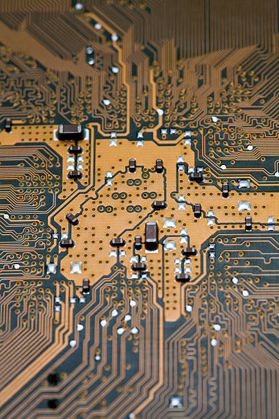
The most important function of impedance control is maintaining Signal Integrity.
When a high-speed signal encounters an impedance discontinuity, part of the signal energy can be reflected toward the source. The reflected signal may interact with the original waveform and produce unwanted effects such as overshoot, undershoot, ringing, and distortion.
These effects can reduce the receiver’s ability to correctly interpret the transmitted data.
In high-speed servers and networking equipment, for example, uncontrolled impedance can contribute to signal-quality problems and communication errors.
Maintaining a consistent transmission-line impedance helps reduce reflections and provides a more predictable signal path.
2.2 Reducing Signal Loss and Transmission Problems
High-speed signals experience various forms of loss as they travel through a PCB.
Impedance mismatch can increase the amount of reflected energy, reducing the energy delivered to the load. This can become increasingly important as transmission speeds and interconnect lengths increase.
A properly engineered Controlled Impedance PCB helps maintain compatibility between the signal source, transmission line, and receiving device.
However, impedance matching alone does not eliminate all high-speed signal losses. PCB designers and manufacturers must also consider conductor loss, dielectric loss, material selection, surface roughness, stack-up configuration, and routing geometry.
This is why impedance control should be integrated into the overall high-speed PCB engineering process.
2.3 Improving Resistance to Crosstalk and Electromagnetic Interference
High-speed PCBs often contain densely routed signal traces. As the spacing between traces decreases and signal frequencies increase, unwanted coupling between neighboring circuits can become more significant.
Proper impedance design and controlled trace geometry help create more predictable electrical characteristics. Combined with appropriate spacing, reference-plane design, grounding, and routing practices, this can help reduce crosstalk and improve overall electromagnetic compatibility.
For industrial control systems and other sensitive applications, stable signal characteristics are particularly important for preventing communication errors and unintended circuit behavior.
3. How Impedance Control Is Implemented During PCB Manufacturing
Impedance control is not limited to a single manufacturing operation. It depends on coordinated control of multiple PCB production stages.
3.1 Selecting the Appropriate PCB Material
The dielectric material has a direct influence on transmission-line impedance.
Different PCB materials have different dielectric constants and loss characteristics. Even variations within the same material system can influence the final impedance if they change the effective dielectric thickness or electrical properties.
For high-speed applications, material selection should therefore consider:
- Dielectric constant and its stability
- Dissipation factor
- Dielectric thickness
- Thermal characteristics
- Frequency requirements
- Manufacturing compatibility
The selected material should be compatible with both the electrical requirements of the design and the manufacturer’s fabrication process.
3.2 Controlling Trace Width and Copper Thickness
Trace geometry is one of the most important manufacturing factors affecting impedance.
For a given PCB stack-up, changes in trace width or copper thickness can alter the characteristic impedance.
During PCB fabrication, etching must therefore be carefully controlled to maintain the designed trace dimensions.
Over-etching can make traces narrower than intended, while under-etching can leave excessive copper. Either condition may cause the actual impedance to deviate from the target value.
Copper thickness must also be controlled consistently across the board because variations can affect transmission-line geometry.
For high-density and high-speed designs, this makes accurate circuit formation an essential part of High-Speed PCB Manufacturing.
3.3 Maintaining Consistent Dielectric Thickness
The distance between a signal trace and its reference plane is another critical impedance parameter.
If dielectric thickness changes, the electrical relationship between the signal conductor and reference plane changes as well. This can cause impedance variation along the transmission path.
The lamination process therefore plays an important role in maintaining consistent dielectric thickness.
Lamination pressure, temperature, time, material characteristics, resin flow, and stack-up configuration should all be considered when establishing the manufacturing process.
A well-controlled lamination process helps maintain a stable multilayer structure and reduces unnecessary impedance variation.
4. The Role of PCB Stack-Up Design
A carefully engineered stack-up is fundamental to achieving predictable impedance.
Before manufacturing begins, designers should define the relationship between signal layers, reference planes, power planes, and dielectric layers.
Important stack-up considerations include:
- Signal-to-plane spacing
- Dielectric thickness
- Copper thickness
- Controlled-impedance trace width
- Differential-pair geometry
- Layer-to-layer registration
- Material dielectric characteristics
For multilayer PCBs, even a small change in the stack-up can affect the impedance calculation.
Therefore, the PCB design should be reviewed together with the manufacturer’s actual material and fabrication capabilities rather than relying solely on nominal design values.
Customers working on complex board layouts can also use GOPCBA PCB Design and Layout Services to coordinate high-speed routing and manufacturing considerations.
5. Impedance Control Across the PCB Manufacturing Process
5.1 Material Preparation
Incoming materials should be checked against the approved material specifications.
Important characteristics may include dielectric thickness, copper thickness, material type, and relevant electrical properties.
Consistent material preparation provides a reliable foundation for subsequent impedance control.
5.2 Inner-Layer Circuit Formation
For multilayer boards, the geometry of inner-layer signal traces must be accurately formed.
Etching parameters should be controlled to maintain the required trace width and spacing. Layer registration should also be monitored to ensure that signal traces remain correctly positioned relative to their reference planes.
5.3 Lamination
During lamination, multiple PCB layers are bonded together into the final multilayer structure.
The lamination process affects dielectric thickness, layer alignment, resin distribution, and overall dimensional stability.
Poor control can lead to variations in the transmission-line structure and consequently affect impedance.
5.4 Outer-Layer Processing
Outer-layer circuit formation must maintain the required trace geometry after plating and etching.
Copper plating thickness should be controlled because the final conductor dimensions can influence the electrical characteristics of high-speed traces.
5.5 Final Inspection and Testing
After fabrication, impedance-related characteristics should be verified using appropriate inspection and testing methods.
Depending on the PCB design and customer requirements, manufacturers may use impedance testing together with dimensional inspection, electrical testing, visual inspection, and other quality-control procedures.
The objective is to confirm that critical transmission lines remain within their specified impedance tolerance.
6. Impedance Control for Different High-Speed Applications
6.1 Data Center and Server PCBs
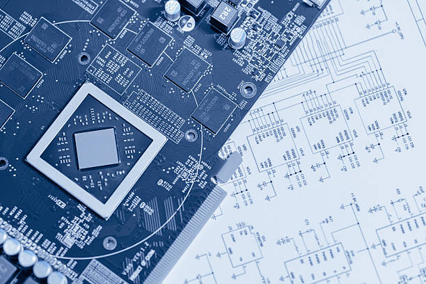
Modern servers rely on high-speed interfaces for communication between processors, memory, storage devices, networking components, and other subsystems.
As signal speeds increase, stable impedance becomes increasingly important for maintaining reliable communication.
PCB stack-up, material selection, differential-pair routing, trace geometry, and connector transitions should therefore be considered together.
6.2 5G and Telecommunications Equipment
5G systems contain high-frequency RF and high-speed digital circuits.
Stable impedance is essential for maintaining predictable signal transmission through RF and high-speed interconnects.
The PCB design must consider transmission-line geometry, dielectric properties, copper characteristics, and surface finishing according to the specific operating frequency and application requirements.
6.3 Industrial Control Systems
Industrial control equipment may combine high-speed communication circuits with power electronics and other electrically noisy systems.
Stable impedance, controlled routing, appropriate grounding, and adequate separation between sensitive and high-power circuits can help improve signal reliability.
A controlled manufacturing process is particularly important when consistent performance is required across multiple production batches.
7. How to Build a Reliable Controlled Impedance PCB
A reliable Controlled Impedance PCB requires collaboration between PCB designers, engineers, and manufacturers.
The recommended workflow includes:
- Define the target impedance requirements.
- Select appropriate PCB materials.
- Develop the stack-up according to electrical requirements.
- Calculate the required trace geometry.
- Review design manufacturability.
- Control material and process parameters during fabrication.
- Monitor trace dimensions and dielectric thickness.
- Perform appropriate impedance and electrical testing.
- Verify the finished PCB against the approved specifications.
For projects that require both PCB fabrication and assembly, GOPCBA Turnkey PCB Assembly Services can integrate PCB fabrication, component sourcing, assembly, inspection, and testing into one coordinated production process.
For prototype-stage development, GOPCBA Prototype PCB Assembly Services can also support engineering validation before moving into larger production volumes.
8. Common Challenges in Impedance Control
Although impedance control is a standard requirement for many high-speed designs, achieving consistent results can be challenging.
Common issues include:
Material Variations
Variations in dielectric properties or thickness can affect impedance calculations and actual production results.
Etching Variation
Differences in trace width caused by etching conditions can change the impedance of critical transmission lines.
Lamination Variation
Changes in resin flow, pressure, temperature, or material thickness can influence the final dielectric structure.
Layer Registration
Misalignment between signal layers and reference planes can affect the intended transmission-line geometry.
Copper Thickness Variation
Differences in plated or etched copper thickness can change conductor dimensions and electrical performance.
These challenges demonstrate why impedance control must be treated as a complete manufacturing discipline rather than a single inspection item.
Conclusion
Impedance Control is one of the fundamental requirements of modern High-Speed PCB Manufacturing.
As electronic systems move toward higher data rates and frequencies, uncontrolled impedance can contribute to signal reflections, waveform distortion, transmission losses, and communication instability.
A reliable Controlled Impedance PCB depends on coordinated control of material selection, stack-up design, trace geometry, dielectric thickness, copper thickness, lamination, etching, plating, and testing.
Ultimately, achieving stable Signal Integrity requires close cooperation between PCB design and manufacturing. By integrating electrical requirements with practical process controls from the beginning of the project, manufacturers can produce high-speed PCBs with more predictable performance, consistent quality, and improved reliability.
For advanced electronic products where high-speed signal transmission is critical, impedance control should not be treated as an optional manufacturing consideration. It should be built into the PCB design and production process from the very beginning.