High-Speed High-Frequency PCB Manufacturing: Key Material and Process Control Considerations
As electronic products continue to evolve toward higher data rates, higher operating frequencies, greater integration, and smaller form factors, PCB performance has become increasingly important to overall system reliability. In high-speed and high-frequency applications, signal transmission is more sensitive to material properties, impedance variation, dimensional tolerances, and manufacturing defects than in conventional PCB applications.
A reliable High-Speed High-Frequency PCB therefore requires careful coordination between material selection and manufacturing process control. From the dielectric material and copper foil to lamination, etching, surface finishing, and final dimensional processing, every stage can influence signal integrity, electrical performance, and long-term reliability.
This article examines the key considerations for high-speed and high-frequency PCB production and provides a practical framework for achieving consistent manufacturing quality.
1. Material Selection: The Foundation of High-Speed High-Frequency PCB Performance
Materials form the foundation of PCB electrical and mechanical performance. Different material characteristics can directly affect signal transmission speed, insertion loss, impedance stability, thermal resistance, and environmental reliability.
For high-speed applications, material selection should focus on electrical stability, low signal loss, thermal performance, and mechanical reliability.
1.1 Base Material: Prioritize Low Signal Loss and Stable Electrical Properties
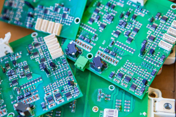
The dielectric material plays a critical role in high-speed signal transmission.
When selecting PCB materials, dielectric constant (Dk) stability is an important consideration. Variations in dielectric constant can change signal propagation characteristics and contribute to impedance variation or signal distortion. These effects become increasingly significant as operating frequencies and data rates increase.
The dissipation factor (Df) is another important parameter. A lower dissipation factor generally indicates lower dielectric loss, helping reduce the amount of signal energy dissipated as heat during transmission.
In addition to electrical properties, the base material should provide sufficient thermal resistance and mechanical strength. High-speed electronic equipment can generate considerable heat during operation. If the PCB material cannot withstand the required thermal conditions, problems such as deformation, delamination, or dimensional instability may occur.
Mechanical strength is also important during PCB fabrication, component assembly, and system integration. A mechanically stable PCB can better maintain its structural integrity under vibration, thermal cycling, and mechanical stress.
For projects requiring specialized materials and advanced fabrication capabilities, GOPCBA PCB Manufacturing Services can support a wide range of PCB material and structural requirements.
1.2 Copper Foil: Focus on Conductivity and Surface Characteristics
Copper foil is the primary conductor responsible for carrying electrical signals through the PCB.
For high-speed and high-frequency applications, copper quality, surface profile, thickness uniformity, and adhesion are important considerations. High-purity copper can help minimize electrical resistance and transmission losses.
Copper surface roughness can also affect high-frequency signal transmission. At higher frequencies, current tends to concentrate near the conductor surface due to the skin effect. Excessive surface roughness can increase the effective signal path and contribute to additional conductor loss.
Copper adhesion is another critical factor. High-speed PCBs may experience temperature fluctuations, vibration, and mechanical stress throughout their service life. Insufficient adhesion between the copper foil and dielectric material can increase the risk of copper peeling, trace damage, and electrical failure.
Therefore, copper foil should be selected according to the application’s electrical, mechanical, thermal, and reliability requirements.
1.3 Solder Mask: Balance Protection and Electrical Compatibility
Solder mask protects exposed PCB circuitry from moisture, dust, chemical contamination, and accidental short circuits. However, in high-speed and high-frequency applications, its electrical characteristics may also need to be considered.
The dielectric properties of the solder mask can influence nearby transmission lines, particularly when traces are routed close to the PCB surface. Excessive or inconsistent dielectric characteristics may affect impedance and signal behavior.
A suitable solder mask should therefore provide stable dielectric properties, low electrical loss, good thermal resistance, and reliable curing performance.
Uniform curing is also important. A properly cured solder mask forms a stable protective layer that helps protect copper traces throughout assembly and long-term operation.
2. Manufacturing Process Control: The Key to High-Speed PCB Quality
Selecting appropriate materials is only the first step. Manufacturing process control ultimately determines whether the selected materials can deliver their intended electrical and mechanical performance.
For high-speed High-Frequency PCB Manufacturing, process parameters must be carefully controlled throughout lamination, circuit formation, surface finishing, and final machining.
2.1 Lamination: Maintain Stable Layer Bonding and Thickness Uniformity
Lamination combines the dielectric materials, copper foils, and other PCB layers into a multilayer structure.
The lamination process has a direct impact on dielectric thickness, interlayer bonding, dimensional stability, and signal integrity.
Temperature, pressure, and time should be controlled according to the selected material system and stack-up design.
Insufficient pressure can result in poor bonding, voids, or delamination. Improper temperature or heating and cooling profiles may affect resin flow, bonding strength, and dielectric characteristics.
Thickness uniformity is particularly important for controlled-impedance applications. Variations in dielectric thickness can change transmission-line geometry and consequently affect impedance.
A carefully engineered lamination process can help maintain consistent layer thickness and stable electrical characteristics across the PCB.
2.2 Etching: Precisely Control Trace Geometry
Etching converts the copper foil into the required circuit pattern. Trace width, spacing, edge quality, and dimensional accuracy can all influence high-speed signal performance.
Over-etching can make traces narrower than intended, increasing resistance and potentially changing impedance. Under-etching can leave excess copper, reducing spacing and increasing the risk of electrical shorts.
Etching uniformity is therefore essential.
Process parameters such as etchant concentration, temperature, spray pressure, and line speed should be monitored and adjusted to maintain consistent circuit geometry.
For high-speed designs, trace width and spacing should be controlled according to the intended stack-up and impedance requirements rather than treated as independent manufacturing parameters.
2.3 Surface Finishing: Balance Solderability and Electrical Performance
Surface finishing protects exposed copper from oxidation while providing a suitable surface for component soldering.
Different surface finishes may be selected depending on the application, assembly process, storage requirements, and reliability expectations.
For example, ENIG can provide good solderability, corrosion resistance, and a relatively flat surface. However, coating thickness and uniformity should be carefully controlled.
OSP provides a thin organic protective coating and can be suitable for applications where cost efficiency and a relatively simple surface structure are important. The coating must be applied uniformly to provide adequate copper protection.
Regardless of the selected surface finish, contamination, oxidation, uneven coating, and other surface defects should be controlled because they can affect soldering quality and long-term electrical reliability.
For customers who need PCB fabrication combined with electronic assembly, GOPCBA Turnkey PCB Assembly Services can integrate PCB manufacturing, component sourcing, assembly, inspection, and testing into a coordinated production workflow.
2.4 Mechanical Processing: Maintain Dimensional Accuracy and Edge Quality
The final machining process determines the PCB’s external dimensions, cutouts, slots, and other mechanical features.
Dimensional accuracy is important for ensuring that the PCB fits correctly into its intended enclosure or electronic system. Excessive dimensional deviation can create assembly interference or mechanical stress.
Edge quality also matters. Burrs, chips, exposed copper, or mechanical damage can create potential reliability problems, particularly in demanding operating environments.
High-precision routing, drilling, laser processing, or other appropriate machining methods should be selected according to the PCB structure and design requirements.
After mechanical processing, the board should be thoroughly cleaned to remove dust, machining debris, and other contaminants.
3. Key Factors for Reliable High-Speed High-Frequency PCB Manufacturing
High-speed PCB production should be managed as an integrated engineering process rather than as a collection of independent manufacturing steps.
Several factors should be considered throughout the project:
- Material selection: Match dielectric and conductor materials to frequency, loss, thermal, and reliability requirements.
- Stack-up design: Establish appropriate signal, reference, dielectric, and copper-layer relationships.
- Impedance control: Maintain consistent trace geometry and dielectric thickness to achieve the required impedance.
- Lamination control: Maintain stable bonding, resin distribution, and dielectric thickness.
- Circuit formation: Control trace width, spacing, edge quality, and etching uniformity.
- Surface finishing: Select an appropriate finish according to solderability, reliability, and application requirements.
- Dimensional control: Maintain accurate board dimensions, holes, slots, and mechanical features.
- Inspection and testing: Establish suitable electrical, dimensional, and visual inspection procedures.
For early-stage product development, GOPCBA Prototype PCB Assembly Services can help engineers validate PCB designs and assembly performance before moving into larger production volumes.
4. Why Process Consistency Matters for High-Speed PCBs
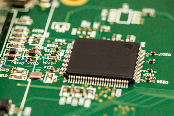
High-speed and high-frequency PCB performance is highly dependent on consistency.
A PCB may meet its basic electrical requirements during initial design, but variations introduced during manufacturing can affect actual signal behavior. Small changes in trace width, dielectric thickness, copper geometry, layer registration, or material characteristics can influence impedance and signal integrity.
For this reason, manufacturers should establish controlled process parameters and monitor critical manufacturing characteristics throughout production.
Quality management should include incoming material inspection, process monitoring, dimensional inspection, electrical testing, and final product verification.
For larger production requirements, GOPCBA High-Volume PCB Assembly Services can support the transition from validated designs to consistent production while maintaining controlled assembly and quality requirements.
5. Integrating PCB Design and Manufacturing
A reliable high-speed PCB cannot be achieved through manufacturing controls alone. PCB design and fabrication must be considered together from the beginning of the project.
Engineers should define the required operating frequency, signal speed, impedance targets, material characteristics, stack-up structure, trace geometry, and manufacturing tolerances during the design stage.
Manufacturing feasibility should also be reviewed before production. Features that are theoretically possible but difficult to manufacture consistently may increase production risk and cost.
A design-for-manufacturing approach can help identify potential problems early and improve the transition from engineering prototypes to production.
GOPCBA also provides PCB Design and Layout Services to help coordinate PCB layout considerations with fabrication and assembly requirements.
6. Building a Reliable High-Speed High-Frequency PCB Solution
High-speed and high-frequency PCB manufacturing is a systematic engineering process in which material selection and process control complement each other.
The right dielectric material can provide a stable electrical foundation, while appropriate copper foil, solder mask, and surface finishing can further support signal integrity and long-term reliability.
At the manufacturing level, precise lamination, controlled etching, appropriate surface finishing, accurate mechanical processing, and comprehensive inspection are all essential for maintaining consistent PCB performance.
The objective should be to minimize signal loss, maintain impedance stability, protect the PCB structure, and achieve reliable performance throughout the product’s expected operating life.
Conclusion
The manufacturing of a High-Speed High-Frequency PCB requires much more than simply selecting a high-performance material.
Electrical properties, thermal characteristics, mechanical strength, copper surface quality, dielectric thickness, trace geometry, lamination parameters, surface finishing, and dimensional accuracy all contribute to the final PCB performance.
By establishing a controlled PCB Manufacturing Process, manufacturers can better translate material and design advantages into stable, repeatable production results.
For applications such as telecommunications, high-speed computing, automotive electronics, RF equipment, networking systems, and other advanced electronic products, close coordination between PCB design, materials, fabrication, assembly, testing, and quality management is essential.
With an integrated approach to engineering and manufacturing, GOPCBA helps customers develop reliable PCB solutions for increasingly demanding high-speed and high-frequency electronic applications.