How to Choose the Right PCB Layer Count: From 1-Layer to 40-Layer PCBs
The number of PCB layers directly affects a circuit board’s routing capacity, signal integrity, power distribution, physical size, reliability, and manufacturing cost. From simple single-layer boards to complex 40-layer designs, PCB layer count should never be selected simply because a higher layer count appears to offer better performance.
Instead, the optimal layer count depends on the actual requirements of the electronic product, including circuit complexity, signal speed, component density, power distribution, electromagnetic compatibility, mechanical constraints, and production cost.
For engineers and product developers, understanding how to determine the appropriate PCB Layer Count can help achieve the right balance between electrical performance, manufacturability, reliability, and cost.
1–2 Layer PCBs: A Practical Choice for Simple Circuits
Single- and double-layer PCBs are suitable for relatively simple electronic designs where routing requirements are limited and advanced signal-integrity performance is not the primary concern.
1-Layer PCB
A single-layer PCB contains conductive circuitry primarily on one side of the substrate. Because the routing structure is simple, it is typically used for applications with relatively low circuit complexity and limited interconnections.
Typical applications may include:
- Simple sensor circuits
- Basic control boards
- Small electronic toys
- Simple power circuits
- Low-complexity consumer electronics
The main advantage of a single-layer PCB is its low manufacturing cost and relatively simple production process.
When the circuit does not require complex routing or extensive component interconnection, adding more layers may provide little practical benefit.
2-Layer PCB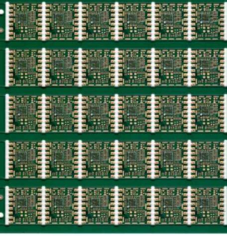
A two-layer PCB uses conductive layers on both sides of the board. Vias allow electrical connections between the two layers, providing significantly more routing flexibility than a single-layer design.
Two-layer boards are commonly used in:
- Small household appliances
- Basic industrial control circuits
- Simple instrumentation
- Power management circuits
- Consumer electronic products
A 2-layer PCB is often an effective compromise when a single-layer board cannot provide sufficient routing space but a multilayer structure would add unnecessary cost and complexity.
4–6 Layer PCBs: Balancing Performance and Cost
As circuit complexity increases, 4- and 6-layer boards provide additional routing space and greater flexibility for separating signal, power, and ground structures.
4-Layer PCB
A typical 4-layer PCB can include signal layers together with dedicated power and ground layers. The exact stack-up depends on the electrical and mechanical requirements of the design.
Compared with a 2-layer PCB, a 4-layer structure can provide:
- More routing space
- Better power distribution
- Improved grounding options
- Shorter return-current paths
- Better control of electromagnetic interference
- Greater flexibility for component placement
Typical applications include small industrial controllers, automotive control modules, consumer electronics, and communication equipment.
When the circuit contains multiple signal groups and requires improved power integrity or signal integrity, a 4-layer board may offer a practical balance between performance and manufacturing cost.
6-Layer PCB
A 6-layer PCB provides additional routing and reference-plane options, allowing engineers to optimize high-speed signals, power distribution, and grounding more effectively.
It can be suitable for applications such as:
- Industrial communication equipment
- Automotive electronic modules
- Smart-home control systems
- Networking devices
- Embedded computing equipment
For designs containing multiple high-speed interfaces or higher component density, moving from 4 layers to 6 layers can provide additional design flexibility without the complexity associated with very high layer counts.
For projects requiring professional stack-up planning and routing optimization, GOPCBA PCB Design and Layout Services can help engineers evaluate layer structures according to the electrical and mechanical requirements of the product.
8–12 Layer PCBs: Supporting More Complex Electronic Systems
When a design incorporates multiple high-speed interfaces, dense component placement, complex power networks, or increasingly demanding signal-integrity requirements, 8- to 12-layer PCBs become more practical.
8-Layer PCB
An 8-layer structure provides significantly more flexibility for separating different signal groups and establishing controlled reference planes.
This can be particularly useful for:
- High-speed networking equipment
- Industrial control systems
- Automotive electronics
- Communication modules
- Embedded computing systems
With a carefully engineered stack-up, high-speed signal layers can be positioned adjacent to appropriate reference planes, helping engineers manage impedance, return paths, crosstalk, and electromagnetic compatibility.
For high-speed designs, however, simply increasing the number of layers does not automatically guarantee better signal integrity. Stack-up configuration, material selection, trace geometry, routing strategy, and power integrity all remain important.
12-Layer PCB
A 12-layer PCB provides still greater routing density and more opportunities to separate signal, power, and ground structures.
Typical applications may include:
- Advanced industrial controllers
- Automotive domain controllers
- High-performance communication equipment
- Networking and switching systems
- Complex computing hardware
At this stage, the PCB Design process becomes increasingly important. Engineers need to consider stack-up design, controlled impedance, thermal management, power integrity, signal integrity, via structures, and manufacturability at the same time.
14–20 Layer PCBs: For High-Performance and High-Density Electronics
When electronic products must accommodate large numbers of components, multiple high-speed interfaces, complex power networks, or strict space constraints, 14- to 20-layer PCBs can provide the routing capacity required by the design.
These boards may be used in advanced:
- Communication systems
- Computing platforms
- Automotive electronics
- Industrial equipment
- High-performance embedded systems
- Networking hardware
At this level, the primary objective is usually not simply to minimize PCB cost. Engineers must determine the layer count needed to achieve the required electrical performance and physical architecture.
Why More Layers May Be Necessary
Higher layer counts can provide more dedicated routing and reference-plane resources. This can help designers:
- Separate sensitive and noisy circuits
- Provide stable reference planes
- Improve power distribution
- Route dense BGA devices
- Accommodate multiple high-speed interfaces
- Reduce excessive routing congestion
- Maintain appropriate signal return paths
However, increasing layer count also increases fabrication complexity and can affect board thickness, material usage, drilling requirements, lamination cycles, and overall production cost.
Therefore, the goal should be to select the minimum practical layer count that satisfies the technical requirements, rather than automatically choosing the maximum available layer count.
22–30 Layer PCBs: Advanced and Specialized Applications
PCB designs in the 22- to 30-layer range are generally associated with highly complex systems requiring substantial routing density, multiple power domains, advanced signal management, and strict reliability requirements.
Potential applications include:
- Advanced aerospace electronics
- High-end medical equipment
- Complex telecommunications systems
- High-performance computing
- Specialized instrumentation
- Advanced industrial control systems
High-Density Routing
As the number of components and high-speed interfaces increases, routing becomes increasingly difficult. More PCB layers can provide additional vertical routing resources and make it possible to separate different functional circuits.
This is particularly useful when a board contains dense BGA packages, multiple power rails, high-speed differential pairs, and sensitive analog circuits.
Reliability and Manufacturing Considerations
High-layer-count boards require careful control of:
- Layer registration
- Lamination
- Via structures
- Plating
- Material selection
- Impedance
- Thermal expansion
- Board thickness
- Electrical testing
At this level, PCB Manufacturing capability becomes an important factor in determining whether a proposed stack-up can be manufactured consistently.
GOPCBA provides PCB fabrication capabilities for complex board structures and can support projects ranging from prototypes to production quantities. GOPCBA PCB Manufacturing Services
32–40 Layer PCBs: Extremely Complex High-Density Designs
Boards with 32 to 40 layers represent the high end of conventional multilayer PCB complexity. They are generally developed for systems where extremely high routing density, complex power distribution, multiple functional blocks, or strict mechanical constraints make lower-layer designs impractical.
Potential applications can include:
- Advanced computing systems
- Aerospace and satellite electronics
- Complex communication infrastructure
- Specialized scientific instruments
- High-end data acquisition systems
- Advanced radar and signal-processing equipment
Extremely High Routing Density
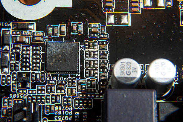
A very high layer count allows designers to distribute large numbers of signals across multiple dedicated routing layers.
This can be particularly valuable when the design includes:
- Large BGA packages
- Multiple high-speed interfaces
- Large numbers of power rails
- High-speed memory
- Dense control circuitry
- Sensitive analog and digital sections
Rather than forcing all signals into a limited number of layers, engineers can distribute routing and reference structures throughout the stack-up.
Advanced Signal and Power Management
Complex computing, communication, and scientific systems may require careful separation of high-speed digital signals, analog signals, clocks, power distribution, and sensitive interfaces.
A properly engineered multilayer stack-up can provide dedicated reference planes and routing layers, helping engineers manage signal return paths and power distribution.
At the same time, a 32- or 40-layer PCB is not automatically better than a lower-layer board. If the design can meet its requirements with fewer layers, a lower-layer structure may provide advantages in cost, manufacturability, and supply-chain flexibility.
How to Determine the Right PCB Layer Count
The most appropriate layer count should be determined from the complete electrical and mechanical requirements rather than from the application category alone.
1. Circuit Complexity
The first question is how many signals, components, and functional blocks must be routed.
Simple circuits may work well with 1 or 2 layers, while increasingly complex systems may require 4, 6, 8, or more layers.
2. Signal Speed and Signal Integrity
High-speed interfaces require careful control of routing geometry, impedance, reference planes, and return paths.
If the design includes high-speed memory, high-speed networking, RF signals, or other sensitive interfaces, additional layers may provide greater flexibility for signal and reference-plane management.
3. Component Density
Dense packages such as BGAs require substantial routing resources.
When component density increases, additional PCB layers can provide more routing channels and help avoid excessive trace congestion.
4. Power Distribution
Modern electronic systems may contain multiple voltage rails and high-current power sections.
Dedicated power and ground structures can improve power-distribution design and provide stable reference planes for sensitive signals.
5. Board Size and Mechanical Constraints
If the available PCB area is limited, increasing the layer count may allow more circuitry to be integrated into the same physical footprint.
This is one reason multilayer boards are widely used in compact electronic products.
6. EMI and EMC Requirements
Electromagnetic compatibility should also be considered during layer-count selection.
A multilayer structure can provide better opportunities for ground-plane design, signal isolation, and controlled return paths. However, EMI performance depends on the complete PCB layout and system architecture rather than layer count alone.
7. Manufacturing Cost
Every additional PCB layer can increase manufacturing complexity and cost.
Therefore, engineers should evaluate:
- Material requirements
- Lamination cycles
- Drilling complexity
- Via technology
- Board thickness
- Fabrication tolerances
- Production volume
- Testing requirements
The most economical solution is generally not the board with the fewest layers, but the board that achieves the required performance with an efficient and manufacturable stack-up.
PCB Layer Count Selection Guide
| PCB Layer Count | Typical Design Complexity | Common Applications | Primary Considerations |
|---|---|---|---|
| 1 Layer | Very low | Simple controls, basic circuits | Lowest cost, simple routing |
| 2 Layers | Low | Consumer electronics, small controllers | Cost and routing balance |
| 4 Layers | Moderate | Industrial controls, automotive modules | Signal and power integrity |
| 6 Layers | Moderate to high | Networking, smart devices, embedded systems | More routing and reference-plane options |
| 8 Layers | High | Communication and computing equipment | High-speed routing and functional separation |
| 10–12 Layers | High | Advanced industrial and automotive systems | Density, SI/PI, power distribution |
| 14–20 Layers | Very high | High-performance electronics | Dense routing and complex power networks |
| 22–30 Layers | Extremely high | Specialized computing, medical, aerospace | Advanced manufacturing and reliability |
| 32–40 Layers | Extreme | Advanced computing, aerospace, scientific systems | Maximum density and complex stack-up |
The ranges above are general design guidance. Actual layer count should be determined from the specific schematic, routing requirements, component packages, electrical performance targets, mechanical constraints, and manufacturing capabilities.
From PCB Design to Production: Why Manufacturability Matters
Choosing the layer count is only one part of developing a successful multilayer PCB.
Once the stack-up has been established, engineers must ensure that the proposed structure can be fabricated consistently. This includes evaluating:
- Material availability
- Copper thickness
- Dielectric thickness
- Trace and spacing requirements
- Via technology
- Aspect ratio
- Lamination structure
- Controlled impedance
- Surface finish
- Electrical testing
For projects that involve both PCB fabrication and component assembly, integrating manufacturing planning early can reduce redesigns and production risks.
GOPCBA supports prototype and production PCB assembly, allowing engineers to validate designs before scaling to larger production quantities. GOPCBA Rapid PCBA Prototyping Services
For complete manufacturing requirements, GOPCBA Turnkey PCB Assembly Services can integrate PCB fabrication, component sourcing, assembly, inspection, and testing into one manufacturing workflow.
Conclusion
There is no universal PCB layer count that is ideal for every electronic product.
A 1- or 2-layer PCB may be the best solution for a simple circuit, while a 4- or 6-layer board can provide a practical balance for moderately complex electronics. More demanding designs may require 8, 12, 16, 20, or even 30+ layers to accommodate high component density, complex power distribution, high-speed interfaces, and strict mechanical constraints.
The key is to select the PCB Layer Count according to the actual technical requirements rather than assuming that more layers always mean better performance.
A well-designed Multilayer PCB should balance electrical performance, signal integrity, power distribution, thermal behavior, mechanical requirements, reliability, manufacturability, and cost.
For engineers developing complex electronic products, early collaboration between PCB design and manufacturing teams is one of the most effective ways to determine an appropriate stack-up and avoid unnecessary redesigns during production.