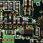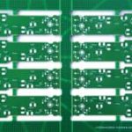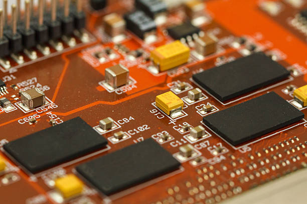
Industrial Robot PCB Requirements: How Multilayer Boards and Resin-Filled Vias Improve Reliability
Industrial robots are evolving toward higher precision, greater payload capacity, faster motion, and longer operating lifespans. As a result, the PCB assemblies used inside robotic controllers, joints, sensors, motor drives, and communication modules face increasingly demanding requirements.
An industrial robot PCB must handle complex signal transmission and power distribution while operating in environments exposed to vibration, oil, dust, temperature fluctuations, and continuous mechanical movement. Conventional PCB structures may not provide sufficient routing capacity or environmental protection for these advanced applications.
The combination of Multilayer PCB technology and Resin-Filled Vias provides an effective solution. Multilayer structures create additional routing space and allow signal, power, and ground networks to be better organized, while resin-filled vias can improve via protection, surface flatness, and structural reliability.
1. Why Industrial Robot PCB Requirements Are Increasing

The expansion of industrial robot applications is driving PCB requirements beyond basic electrical connectivity. Modern robotic systems increasingly require high signal integrity, compact designs, high current capability, and long-term reliability.
1.1 Supporting Both High-Speed Signals and Power
Modern industrial robots may integrate machine vision, force sensing, position feedback, multi-axis motion control, and motor-drive systems.
These functions can require different types of electrical signals to coexist on the same PCB. High-speed control and sensor signals may need to be routed alongside higher-current power circuits.
If these networks are not properly separated and controlled, unwanted coupling and noise can affect signal quality and system performance. A well-designed PCB therefore needs appropriate layer allocation, grounding, routing, and power distribution.
For projects requiring controlled routing and optimized board structures, professional PCB design and layout services can help establish a manufacturable design before fabrication begins.
1.2 More Components in Smaller Spaces
Industrial robot joints, arms, controllers, and end-effectors are becoming increasingly compact. At the same time, more electronic functions are being integrated into limited physical spaces.
Sensors, processors, communication interfaces, motor drivers, connectors, and power-management components may all need to fit within a relatively small PCB area.
A multilayer structure provides additional internal routing layers, allowing designers to distribute circuits vertically rather than relying entirely on the top and bottom surfaces. This can significantly improve routing flexibility and component density.
1.3 Long-Term Operation in Harsh Industrial Environments
Industrial robots commonly operate in manufacturing environments where PCBs may be exposed to continuous vibration, dust, oil, cooling fluids, and temperature cycling.
These conditions can place additional stress on solder joints, vias, copper structures, and PCB materials. Therefore, PCB reliability cannot be evaluated solely from electrical performance. Mechanical strength, thermal stability, environmental resistance, and manufacturing consistency also need to be considered.
2. How Multilayer PCBs Meet Industrial Robot Requirements
A Multilayer PCB uses multiple conductive layers separated by dielectric materials. This structure provides considerably more routing capacity than a conventional single- or double-sided PCB.
2.1 Better Separation of Signal, Power, and Ground
One of the major advantages of multilayer construction is the ability to assign different layers to different electrical functions.
For example, a PCB stack-up may include dedicated signal layers, power planes, and ground planes. This allows high-speed signal traces and high-current power networks to be physically separated where appropriate.
A continuous reference plane can also provide a more controlled return-current path, which is important for maintaining signal integrity and reducing unwanted coupling.
However, layer assignment should be determined according to the actual circuit, stack-up, impedance requirements, power distribution, and mechanical constraints rather than simply increasing the number of layers.
2.2 Higher Routing Density in Compact Designs
Multilayer construction allows connections to pass between layers through vias, reducing the need to route every connection across the external PCB surfaces.
This is particularly useful for compact robotic assemblies where board area is limited but component density is high.
Depending on the circuit complexity, a design may use four, six, eight, or more layers. The optimal layer count should balance routing requirements, signal integrity, thermal considerations, manufacturability, and cost.
For projects that need to move efficiently from design into fabrication, GOPCBA PCB manufacturing services support PCB production for different layer counts, materials, and advanced interconnection structures.
2.3 Improved Structural Performance
Multilayer PCBs are manufactured through controlled lamination processes that bond multiple dielectric and copper layers into a single board structure.
A properly designed and manufactured multilayer board can provide the structural rigidity required by many industrial electronic assemblies. This can be especially valuable in applications subject to continuous mechanical vibration.
Nevertheless, PCB durability depends on the complete material and manufacturing system, including laminate selection, copper structure, hole quality, lamination control, soldering processes, and final inspection.
3. Resin-Filled Vias: Additional Protection for Multilayer PCBs
Although vias are essential for multilayer interconnection, certain via structures can create challenges in applications where contamination, mechanical stress, or surface flatness are important.
Resin-Filled Vias address some of these challenges by filling selected via holes with insulating resin and subsequently processing the surface to create a more uniform structure.
3.1 Protecting Via Structures
Open or improperly protected via structures can potentially become pathways for contaminants in demanding environments.
In industrial applications, oil, dust, moisture, and other contaminants may create reliability concerns if PCB structures are not properly protected.
Resin filling can close the internal void of a selected via, helping reduce exposure and providing additional protection around the interconnection structure.
For example, in a robotic joint exposed to lubricants and continuous movement, appropriate via filling and surface treatment can contribute to a more robust PCB structure.
3.2 Improving Mechanical Reliability
Industrial robots frequently perform repetitive, high-speed movements. Their electronic assemblies may therefore experience continuous mechanical stress.
Properly implemented resin-filled vias can provide additional mechanical support around the via structure. This can be beneficial where via reliability is a concern, although the actual performance depends on the resin system, hole geometry, copper plating, thermal cycling, and overall PCB construction.
For applications with demanding reliability requirements, PCB fabrication should be evaluated together with assembly and testing rather than treating the via process as an isolated feature.
3.3 Creating a More Uniform PCB Surface
A major benefit of via filling is the ability to create a flatter PCB surface after subsequent processing.
A controlled, planar surface can be useful for certain component-placement and soldering configurations. It may also reduce mechanical interference between the PCB and nearby components or enclosure structures.
This characteristic becomes particularly valuable in compact robotic electronics where component placement and available clearance are tightly constrained.
4. Multilayer PCB + Resin-Filled Vias: A Combined Reliability Strategy
Multilayer structures and resin-filled vias solve different aspects of industrial robot PCB requirements.
The multilayer structure primarily addresses electrical performance, routing density, power distribution, and compact design. Resin-filled vias provide additional support for via protection, structural robustness, and surface flatness.
When these technologies are appropriately combined, they can help create a PCB architecture better suited to demanding robotic applications.
4.1 Supporting High-Speed Control and Power Circuits
A carefully engineered stack-up can allocate suitable layers for high-speed signals, power distribution, and ground references.
This approach can help maintain predictable signal paths while providing sufficient current-carrying capacity for motor-control and power circuits.
The actual stack-up should be designed according to the required impedance, operating frequency, copper thickness, dielectric construction, and current requirements.
4.2 Improving Environmental Durability
Industrial robots may operate continuously for extended periods. PCB reliability therefore depends on more than the initial electrical performance of the board.
A suitable combination of multilayer construction, via protection, material selection, soldering processes, and surface finishing can help improve resistance to the stresses associated with industrial environments.
For complete production programs, turnkey PCB assembly services can integrate PCB fabrication, component sourcing, SMT assembly, through-hole processing, inspection, and testing into a coordinated manufacturing workflow.
4.3 Supporting Compact Robotic Electronics
Space constraints are becoming increasingly important in robotic joints, controllers, vision systems, and end-effectors.
Multilayer routing enables more connections within a smaller board footprint, while planar via structures can support compact component placement in suitable designs.
This makes the technology particularly relevant to robotic electronics where electrical complexity continues to increase while available installation space remains limited.
5. Key PCB Manufacturing Considerations for Industrial Robots
The successful application of multilayer and resin-filled via technology depends heavily on manufacturing process control.
Important factors include:
- Material selection and dielectric construction
- PCB layer stack-up design
- Controlled impedance requirements
- Copper thickness and current-carrying capability
- Via drilling and plating quality
- Resin filling and curing control
- Lamination process consistency
- Surface finishing
- AOI and electrical testing
- Dimensional and visual inspection
- Traceability throughout production
These factors should be considered during the design stage rather than added after PCB fabrication has already begun.
For early-stage robotic projects, rapid PCBA prototyping can help engineers validate PCB design, component placement, assembly processes, and functional performance before moving into larger production volumes.
6. Typical Industrial Robot PCB Applications
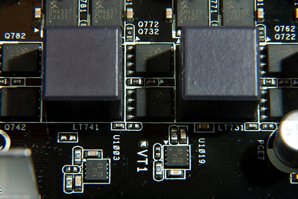
The combination of multilayer construction and advanced via technologies can be considered for a range of robotic electronics, including:
Robotic Controllers
Robot controllers may contain processors, communication interfaces, memory, power circuits, and motion-control electronics. Multilayer routing can provide the density and electrical separation required by these complex systems.
Robotic Joints and Servo Drives
Joint modules and servo-drive electronics can experience significant vibration and thermal cycling. PCB construction and via reliability are therefore important design considerations.
Machine Vision Systems
Vision modules often involve high-speed image data and compact electronic architectures. Controlled routing and appropriate layer structures can help support high-speed signal transmission.
Force and Position Sensors
Sensor interfaces require stable signal acquisition and low-noise electrical environments. Proper grounding, routing, and PCB stack-up design can contribute to reliable sensor performance.
End-of-Arm Tooling
Robotic grippers, welding systems, inspection tools, and other end-effectors often have limited installation space and demanding environmental conditions. Compact multilayer PCB designs can help integrate multiple electronic functions into constrained assemblies.
7. How to Build a Reliable PCB for Industrial Robots
Choosing the right PCB technology should begin with the application requirements rather than a predetermined layer count or manufacturing process.
A reliable development process should consider:
- Define electrical requirements — Identify signal types, operating frequencies, power levels, current requirements, and impedance targets.
- Evaluate mechanical constraints — Confirm board dimensions, thickness, mounting locations, connector positions, and available clearance.
- Develop the stack-up — Allocate signal, power, and ground layers according to electrical and mechanical requirements.
- Evaluate via structures — Determine whether standard vias, blind/buried vias, via filling, or other interconnection technologies are appropriate.
- Select suitable materials — Consider thermal performance, dielectric properties, mechanical strength, and operating environment.
- Review manufacturability — Make sure the design can be consistently fabricated within realistic process tolerances.
- Prototype and test — Validate electrical, mechanical, thermal, and functional performance before volume production.
- Control production quality — Maintain consistent materials, processes, inspection standards, and traceability during production.
For larger production requirements, high-volume PCB assembly can provide a controlled transition from validated prototypes to repeatable production.
Conclusion
The evolution of industrial robots is placing greater demands on the PCBs used in controllers, sensors, servo drives, communication modules, and robotic joints.
A Multilayer PCB provides the routing capacity, layer flexibility, and electrical architecture needed for increasingly complex robotic electronics. Resin-Filled Vias can further improve selected PCB structures by providing via protection, mechanical reinforcement, and improved surface flatness.
Together, these technologies can form an effective PCB strategy for applications that require compact designs, stable signal transmission, reliable power distribution, and long-term operation in demanding industrial environments.
However, technology selection should always be based on the specific electrical, mechanical, thermal, environmental, and manufacturing requirements of the robotic system. A well-engineered PCB design combined with disciplined PCB Manufacturing and assembly quality control is ultimately the foundation of dependable Industrial Robot PCB performance.