Five Key Points of PCB Board Design
Most of what determines whether a board is quiet, manufacturable and easy to build comes down to five decisions that are made before detailed routing begins. None of them is complicated, and all of them are easier to get right at the start than to correct afterward, because each one constrains the choices available later. Working through them in order is a practical way to structure the early part of PCB board design, and each one is easier to satisfy when it is considered before the routing density is fixed.
Orientation and Partitioning
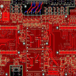
The first decision is where each functional group sits on the board and how the signal flow runs between them. Inputs and outputs, AC and DC sections, strong and weak signals, high and low frequencies, and high and low voltages should each be arranged so that the flow is linear and the groups do not interleave. The purpose is to prevent one group from coupling into another, and the arrangement that achieves it best is a straight line from input to output. A circular arrangement, where the flow returns to its starting point, is the worst case because the input section ends up adjacent to the output section. The requirement is relative rather than absolute: a board with only DC and low-level signals can be laid out much more loosely than one that mixes a switching supply with a sensitive measurement front end.
Choosing the Ground Point
Grounding is where most of the remaining difficulty lives, and there is rarely a single answer that fits every board. The starting principle is that circuits which must share a reference should be joined at a defined point rather than connected by whatever path happens to be shortest. A common arrangement is to bring the returns of a sensitive stage together and then take a single connection to the main ground, so that the sensitive stage does not carry the current of anything else. In practice, physical constraints make the ideal arrangement impossible, and the designer has to choose the compromise that keeps the largest currents out of the most sensitive returns. The structure of those returns is described in this article on ground routing and power trace planning.
<img src="https://www.gopcba.com/wp-content/uploads/2026/09/21-2.jpg" alt="PCB board layout showing partitioned sections and copper pour” />
Placing the Decoupling Capacitor and Filters
A schematic shows the supply filter and decoupling capacitor values but rarely shows where they belong. Their position, not their value, usually determines whether they do anything. A capacitor that is meant to supply the transient current of a switching device or gate must sit as close to that device as the layout allows; a capacitor placed at the far end of the board supplies nothing. The same applies to filter components, whose leads should be short enough that the inductance of the connection does not cancel the intended effect. An interesting consequence of placing these components correctly is that grounding problems become much less noticeable, because the local current loop is closed where the current is drawn rather than somewhere else on the board.
Trace Width, Pads and Copper Pour
Trace width should follow from the current the trace carries and from the impedance the net requires, and wider is generally better where the choice is free. High-voltage and high-frequency routes should be smooth, without sharp corners, and the ground conductor should be as wide as possible, preferably as a large area of copper. Pad and hole sizes need to match each other: a pad that is too small for its hole cannot be drilled reliably, and a mismatch produces a crescent-shaped pad after drilling. Where a signal trace is thin and the surrounding area is empty, the etch will not be balanced, and the thin trace may be attacked more than the surrounding copper and break. Adding copper to the empty areas solves the etching problem and improves the return path at the same time, and the trade-offs between a solid and a meshed fill are covered in this article on copper flooding, mesh or solid.
Via Count and Routing Density
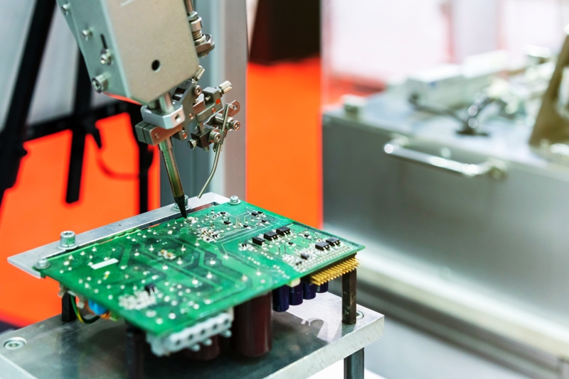
Problems in this area rarely appear during design and frequently appear in production. Every via is a hole that has to be drilled and plated, and a high via count increases the load on the plating process, where incomplete copper deposition inside a deep hole becomes a hidden defect that may not show up until the board is in the field. A layout should therefore use the minimum number of vias consistent with the routing, and identical nets should not be re-routed through additional vias for cosmetic reasons. Routing density deserves the same treatment: traces running in the same direction at a very fine pitch are difficult to solder without bridging, so the density should be set by the capability of the soldering process rather than by the smallest pitch the layout tool allows. The minimum spacing between solder joints should be chosen with the quality and throughput of the assembly operation in mind, because a spacing that is technically possible can still destroy the yield.
Reviewing the Five Points Together
These five decisions interact. Improving the partitioning reduces the grounding problem, placing the decoupling correctly hides what remains of it, a wide ground and balanced copper pour improve both the electrical and the fabrication result, and a lower via count reduces the cost of the whole board. The pad geometry that ties several of them together is described in this article on PCB pad design standards. Reviewing all five before routing starts is a short exercise that pays for itself, and it is far cheaper than discovering at first article that a decision made in the first hour cannot be undone.
Deciding These Points Before the Schematic Is Frozen
Several of the five points can be settled while the schematic is still open, which is the cheapest time to settle them. The partitioning of the board follows from the block diagram, so the question of which sections must be kept apart can be answered before the first component is placed. The ground point and the return structure follow from the same diagram, because the current paths are visible in it. The placement requirements for the decoupling components and filters are also visible, and a note on the schematic that a capacitor belongs physically beside a particular device prevents the question from being raised again during layout. The pad and via decisions follow from the fabricator’s capability, which should be a known input rather than something discovered when the data is released. None of this removes the need to review the layout later, but it removes the most expensive kind of review, which is the one that finds a structural problem after the routing is complete and the schedule has no room left for it.
FAQ
Is a circular signal flow ever acceptable? It is a compromise rather than a goal. Where the mechanical layout forces it, the sections should be physically separated as much as the board allows.
How close does a decoupling capacitor need to be? Close enough that the loop formed with the supply and ground pins is short compared with the wavelength of the highest frequency of concern. In practice, that means beside the pin.
Why reduce the via count if a higher count routes more cleanly? Because every via adds a plating step and a potential hidden defect, so the count should be justified by the routing rather than chosen for appearance.