Base Station PCB Manufacturing: Materials, Process and Assembly
Telecom infrastructure boards sit at the demanding end of mainstream PCB manufacturing. They combine high layer counts, radio frequency sections with tight impedance control, heavy copper for power distribution and a service life measured in decades. The manufacturing sequence reflects all four requirements at once.
What Makes Base Station Boards Different
A base station PCB carries several subsystems on one panel: an RF front end, a digital baseband section and the power conversion that feeds both. Each has a different priority, and the stackup has to satisfy them simultaneously while keeping the board manufacturable at volume.
Reliability expectations add another constraint. Equipment mounted on a tower or in an outdoor cabinet experiences wide temperature swings, humidity and vibration, so the finished assembly must survive thermal cycling that a consumer product never sees.
Material Selection and High Frequency Laminate
The RF section usually dictates the material. Loss tangent and dielectric constant stability matter more than raw strength, and a high frequency laminate with a controlled dielectric constant keeps the impedance predictable across temperature and frequency. The digital section can often use standard FR-4, which keeps cost under control.
Mixing materials in one stackup is common, with the RF layers using the low-loss material and the digital layers using a standard grade. The hybrid construction has to be planned with the fabricator, because the two materials behave differently during lamination and drilling.
Layer Count and Stackup for RF Sections
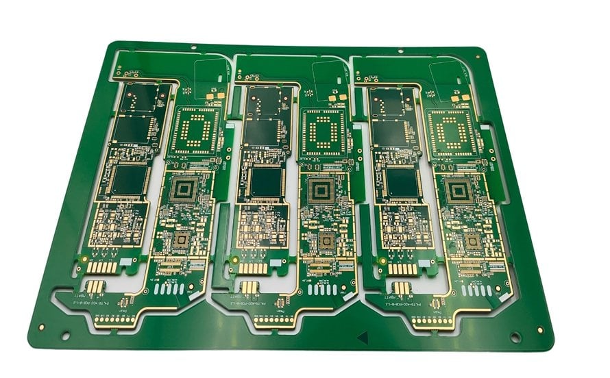
Layer count typically runs high, and the stackup places the RF traces against reference planes with a known dielectric thickness on both sides. Stripline construction is preferred for sensitive RF nets because it is shielded on both faces and less susceptible to crosstalk from adjacent routing.
Grounding is continuous under the RF section, with via stitching around the perimeter to close the cavity. Splits in the ground plane are avoided in this area entirely, since a discontinuity under an RF trace changes the impedance and radiates.
Heavy Copper and Power Distribution
Power amplifier rails draw substantial current, so inner layers carrying those rails use heavier copper than the signal layers. The extra weight affects etching and lamination: heavier copper needs more etch time, which reduces achievable line width, and it needs more resin in the prepreg to fill around the traces.
Thermal relief and copper balance matter as well. Large copper areas adjacent to fine signal layers create resin starvation and lamination voids, and a design that ignores copper balance usually pays for it in yield rather than in function.
Drilling, Plating and Aspect Ratio
Thick boards with many layers push the aspect ratio, and plating uniformity inside a deep barrel is the limiting factor. Sequential lamination with buried vias reduces the depth that must be plated, but adds process steps and cost, so the stackup is usually optimised to keep the deepest plated hole within a comfortable ratio.
Back drilling is common on high-speed nets to remove stubs that would otherwise notch the channel response. The process removes copper from the unused portion of the barrel, and it has to be controlled to a depth that clears the stub without damaging the last connected layer.
Controlled Impedance and Loss Budget
Impedance control on a base station board is not limited to a few differential pairs. RF traces, digital buses and the clock tree may all carry impedance requirements, each with its own tolerance. The fabricator builds coupons for each, and the first article includes a report for the whole set rather than a single measurement.
Loss is a separate calculation. At the frequencies used in modern infrastructure, dielectric loss and copper roughness both contribute, and the loss budget is what decides whether a low-loss material is mandatory or merely helpful. Reviewing high-frequency trace and data bus routing early keeps that decision from being made after the stackup is fixed.
<img src="https://www.gopcba.com/wp-content/uploads/2026/08/Electrical-Testing.jpg" alt="Thermal management features around a power amplifier on a base station PCB” />
Thermal Management Under High Power
Power amplifiers convert a large share of their input to heat, and removing it is a mechanical and electrical problem at once. Thermal vias under the device transfer heat to internal copper and then to a heat sink, and the copper area connected to those vias has to be sized for the power involved rather than for convenience.
Materials matter too. A laminate with a higher glass transition temperature resists the softening that would otherwise let plated barrels crack under repeated thermal cycling, and the assembly is typically qualified with thermal shock testing rather than a single reflow pass.
Assembly and RF Connector Attachment
RF connectors are often soldered to both the signal pad and the surrounding ground, and the joint must maintain a continuous ground path to the board planes. Poor reflow around a connector footprint shows up as an impedance mismatch rather than as an obvious open circuit, which makes first article inspection important.
Large shielded modules, heat spreaders and heavy components need appropriate pad geometry and stiffening. Voids under a thermal pad measurably increase junction temperature, so the paste pattern and reflow profile are part of the design review, not only the process setup. Where the assembly is exposed to moisture or contamination, a conformal coating decision follows.
Testing and Inspection
Testing reflects the cost of failure. Electrical test is standard, impedance coupons are measured for every controlled structure, and microsections verify plating thickness and barrel integrity on a sample basis. RF assemblies frequently add a functional test with network analysis to confirm that the passband and return loss meet the specification.
Inspection of the plating process deserves particular attention, because a barrel defect that survives hundreds of thermal cycles eventually becomes a field failure, and copper plating defect prevention is cheaper than a tower visit. Where high layer counts and fine vias are combined, electroplating and via filling practice determines whether the buried structures remain reliable.
Qualification and Volume Ramp
A base station board rarely goes from first article to volume in one step. Qualification usually includes thermal cycling, humidity exposure and vibration, because the product must survive an outdoor cabinet for years. Each qualification stage can send the design back to the layout, which is why the RF assembly definition and the mechanical interface are frozen as early as possible.
The volume ramp then tests the process rather than the design. Plating uniformity, lamination yield and impedance distribution across a panel become the limiting factors, and the data gathered during the prototype phase is what makes those problems visible before they affect a shipment.
Keeping the same fabrication source through the ramp matters for a board with this many controlled parameters. Changing supplier in the middle of a qualification program resets the evidence that the process holds the specification.
FAQ
Can a base station board use standard FR-4 throughout? Sometimes, particularly for lower frequency products where the loss budget allows it. The decision follows the loss calculation rather than a rule, and mixing a low-loss material only in the RF layers is a common compromise.
Why is back drilling used on these boards? It removes the unused portion of a through via that would otherwise act as a stub and notch the channel response. On thick boards with long vias, that notch can appear within the operating band.
What is the biggest yield risk in this kind of build? Copper balance and lamination quality. Heavy copper next to fine signal layers creates resin starvation at the same time as tight impedance tolerances demand precise dielectric thickness, and the two constraints have to be satisfied in the same stackup.