




PCB Manufacturing Processes: A Guide to the Main Types
A PCB manufacturing process is a sequence of chemical, mechanical and thermal operations that turns a copper-clad laminate into a board with controlled conductors. There are variations for flexible materials, heavy copper, high layer counts and radio frequency substrates, but the core sequence is shared by almost all of them.
Understanding the sequence helps a designer predict which features are easy, which are expensive and which are the source of the defect they are currently chasing.
Step One: Inner Layer Imaging
Inner layers begin as copper-clad laminate coated with a photosensitive resist. The resist is exposed through a film carrying the layer pattern and then developed, leaving resist only where copper should remain.
Photolithography for PCB work is contact printing rather than the projection used in semiconductor fabrication, so resolution is limited by film quality, exposure energy and the gap between film and panel. That is why the practical minimum line width depends on the imaging method and why laser direct imaging gives finer features than conventional exposure.
Step Two: Etching
Etching removes the copper that the resist does not protect. The panel passes through a spray of etchant, and the reaction proceeds from the surface downward and sideways. The lateral removal, described by the etch factor, leaves a trapezoidal trace.
Uniformity across the panel is the main concern. Etch rate varies with spray pressure, panel position and the amount of dissolved copper in the bath, so the process is compensated deliberately: the film is drawn with a correction so that the finished trace lands near its nominal width.
Step Three: Lamination
Multilayer boards are built by stacking inner layers with prepreg between them and pressing the assembly under heat and pressure. The resin in the prepreg flows, fills the copper topography and cures into a solid dielectric.
Lamination determines registration, thickness and the absence of voids. A press cycle that is too fast leaves resin-starved areas or trapped air, which appear later as delamination during reflow. The temperature ramp and the pressure profile are specific to the material system, so material substitution is not a trivial change.
<img src="https://www.gopcba.com/wp-content/uploads/2026/08/PCB-Assembly-Services.jpg.webp" alt="Electroplating line used in PCB manufacturing” />
Step Four: Drilling
Drilling creates the holes that connect layers and that accept through-hole components. Mechanical drilling with carbide bits dominates, with laser drilling used for microvias in high-density boards.
Bit life and entry material control hole quality. A worn bit smears the resin and produces a rough hole wall that plating cannot cover reliably; that condition, known as smear or resin recession, is the origin of many barrel failures. Drill hits are counted and bits replaced on a schedule rather than on appearance.
Hole depth and aspect ratio matter for plating. A high aspect ratio hole, deep and narrow, is harder to plate evenly, which is why fabricators publish a maximum and why designs should stay below it.
Step Five: Plating and Copper Deposition
Plating makes the walls of the holes conductive. A thin electroless copper layer is first deposited chemically, then electroplating thickens it to the required wall thickness. The same electroplating step adds copper to the surface where the pattern requires it.
The plating bath is the most chemistry-sensitive part of the plant. Additive concentrations, current density and agitation determine whether copper fills a via or pinches it, and whether the deposit is ductile enough to survive thermal cycling.
Where vias must be filled, as in via-in-pad designs, plating is followed by conductive or non-conductive plugging and a planarization step so the pad is flat enough for assembly.
Step Six: Outer Layer Imaging and Etching
After plating, the outer layers are patterned with the same imaging and etching sequence used on the inner layers. The pattern is defined against the already-plated holes, so registration between copper and holes is checked here.
Where a design uses a subtractive process on a heavy copper layer, the etch factor becomes significant and trace width tolerance widens. Heavy copper boards are often patterned with a modified process to keep tolerances reasonable.
Step Seven: Solder Mask and Legend
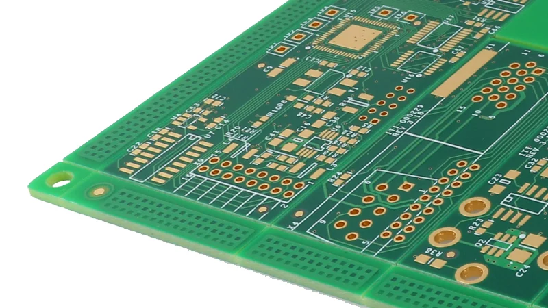
Solder mask is screen printed or curtain coated, then imaged and developed so that it covers everything except the pads. Curing follows, and the cure must balance adhesion against brittleness: an undercured mask lifts during soldering, and an overcured mask cracks during thermal cycling.
The legend is printed last, usually by screen printing with epoxy ink. It carries reference designators and orientation marks, and it should be treated as documentation rather than decoration, since it is the fastest way to locate a component on an assembled board.
Step Eight: Surface Finish
Surface finish protects the exposed copper until soldering. Hot air solder levelling is inexpensive and durable, electroless nickel immersion gold gives a flat surface suitable for fine pitch, immersion silver is cost effective for volume work, and hard gold is used for edge connectors that see wear.
The choice affects shelf life, solder joint quality and cost, and it interacts with assembly: a finish that oxidizes in storage produces wetting problems that no reflow profile can repair.
Special Processes and Their Cost
Some designs need processes beyond the standard sequence, and each of them changes the price and the lead time. Heavy copper plating, controlled depth routing, cavity formation, back-drilling of press-fit holes and sequential lamination for high layer counts all require additional steps and additional handling between them.
Sequential lamination is the clearest example. Layers are pressed in more than one cycle so that buried vias can be formed between them, which means the panel enters the lamination press, the drill and the plating line repeatedly. Cost rises with each cycle, and yield risk rises with it.
Flexible and Rigid-Flex Manufacturing
Flexible circuits follow a different sequence. The base material is polyimide, the conductive pattern is often defined by a combination of imaging and coverlay lamination, and the coverlay replaces solder mask as the protective layer. Adhesive-based and adhesiveless constructions behave differently through bending, and the choice is made on the required bend radius and cycle count.
Rigid-flex boards combine both flows. The flexible cores are processed with the rigid layers and then laminated together, with the bond between the two defining the reliability of the transition. Contamination or voids at that interface produce delamination that appears only after assembly, which makes process control at this step the critical variable.
Traceability and Process Control
Every step in the sequence is monitored with measurements rather than with visual checks alone. Copper thickness is measured on coupons, hole wall quality is checked by microsection, and plating thickness is verified by X-ray fluorescence. Those records are what allow a supplier to explain a deviation instead of guessing at it.
For the designer, the practical implication is that process capability is finite and documented. Reading the supplier capability sheet before layout, rather than after a failed order, is the cheapest way to avoid redesign.
Electrical Test, Inspection and Routing
Finished boards are electrically tested for continuity and isolation, then visually inspected and routed from the production panel. Test fixtures are built from the same netlist used for fabrication, so a netlist error propagates into both the board and the test.
Coupons for impedance measurement are included on the panel, and their results are reported with the shipment. Reviewing that report against the design target is the last checkpoint before the boards reach assembly.
Further reading: electroplating additives, copper plating defect prevention, and layer stackup from one to eight layers.
FAQ
Which process step limits the minimum trace width? Imaging and etching together. Laser direct imaging defines the pattern more accurately than film exposure, and the etch factor then determines how much narrower the finished trace becomes.
Why does hole quality matter so much? Because the plating that follows has to cover the whole barrel. A rough or resin-smeared wall produces an incomplete deposit that survives test but fails after thermal cycling.
Can surface finish be changed without requalifying the board? Usually yes, but the assembly profile and shelf life assumptions must be rechecked. Finishes differ in oxidation behavior, and a joint that formed reliably on one may not form on another.

9 Comments
Low-Cost PCB Production: Design Choices That Cut Price
[…] Related reading: custom PCB cost factors, design guidelines for manufacturable boards, and PCB manufacturing processes. […]
PCB Capture Pad and Annular Ring Design
[…] Related reading: PCB manufacturing tolerances, via in pad versus plated through, high density interconnect PCB, and PCB manufacturing processes. […]
PCB Gold Plating Types and Thickness Guide
[…] reading: PCB manufacturing processes, PCB manufacturing tolerances, lead free versus leaded solder, and PCB design quality […]
Carbon Ink vs Carbon Film PCB Selection
[…] reading: PCB manufacturing processes, PCB manufacturing tolerances, PCB design quality characteristics, and conformal coating and board […]
Via Plugging and Tenting Compared
[…] reading: via in pad versus plated through, PCB manufacturing processes, PCB manufacturing tolerances, and high density interconnect […]
PCB Routing Precision and Outline Tolerance
[…] reading: board outline and mounting design, PCB manufacturing tolerances, PCB manufacturing processes, and PCB capture pad […]
PCB Board Thickness Standard Values
[…] reading: PCB manufacturing tolerances, PCB manufacturing processes, PCB warpage and stackup balance, and multilayer PCB […]
Embedded Copper Coin PCB Guide
[…] Related reading: thermal substrate comparison, trace width and current calculation, metal core PCB thickness, and PCB manufacturing processes. […]
IC Substrate vs PCB Explained
[…] Related reading: high density interconnect PCB, any layer HDI PCB, optical module PCB design, and PCB manufacturing processes. […]