




Rigid-Flex PCB for Wearables: Bend Radius and Stackup Rules
A wearable device folds electronics into a shape that the human body dictates. The display, the sensor package, the battery and the radio rarely sit on one plane, and the space between them is measured in millimetres that also have to move. A rigid-flex PCB solves both problems at once by combining stiff circuit areas with flexible sections that bend into the enclosure.
The price is a design that has to be right the first time, because a flex laminate and its adhesives behave differently from a conventional board. This article covers the mechanical rules, the stackup decisions and the assembly practices that decide whether a wearable rigid-flex survives the wrist it was designed for.
Why Wearables Push Toward Rigid-Flex
A conventional approach uses one rigid board and a separate cable assembly, joined by connectors. Connectors cost height, they add two interfaces that can fail, and they consume the very space the product does not have. A rigid-flex removes those interfaces by making the connection part of the circuit itself.
That integration also improves the electrical performance, because a controlled impedance flex section behaves better than a short cable with a connector at each end. The gain is largest for high speed interfaces and for the sensitive analog lines that a biosensor front end needs.
Bend Radius and Flex Life
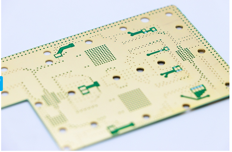
Flex life is governed by strain in the copper, and strain is governed by bend radius and by the position of the copper within the stack. A single layer of rolled annealed copper bent once can accept a radius several times its thickness, while the same copper in a dynamic application that bends thousands of times needs a much larger radius and a much thinner dielectric.
The practical rule is to keep the bend radius above ten times the total flex thickness for a static bend and substantially more for a dynamic one, and to place the neutral axis so that the copper of the critical signal layer is as close to it as the stack allows. Bends should also be spread over a longer section rather than concentrated at one line.
Stackup and Adhesive Selection
A flex stack is built from polyimide film, copper and adhesive or, increasingly, from an adhesiveless construction where the copper is cast or laminated directly onto the film. Adhesive layers are thicker and softer, which helps the mechanical behaviour but restricts the temperature rating and the dimensional stability.
The stackup for a wearable usually combines a two layer flex core in the bend area with bonded rigid sections at the ends. The transition between the two is the most delicate region on the board, so the copper is designed with a gentle taper, the coverlay is kept continuous where possible and no via is placed within the bend.

Copper and Coverlay Design Rules
Copper in a flex is usually rolled annealed rather than electrodeposited, because the grain structure survives bending better. Conductors run perpendicular to the bend line where the layout allows, traces are kept uniform in width and spacing, and any change of direction is made with a curve rather than an abrupt corner.
The coverlay protects the conductors and defines the mechanical surface of the flex. It is patterned with the same care as the copper: openings are kept away from the bend, the adhesive is chosen to match the flex life requirement, and stiffeners are added only where a component or a connector has to be supported.
Assembly, Test and Handling
Flexible circuits are assembled the same way as rigid boards, with one important difference: the panels are thinner and more prone to handling damage, so fixtures, carriers and reflow support matter more. Components near a bend are avoided, and where they are unavoidable, the bend is moved rather than the component.
Test access should be designed in, because probing a flex after assembly is difficult. Test pads on the rigid ends, a defined flexing cycle for qualification and a mechanical simulation that includes the enclosure help to catch the failure modes that a functional test at room temperature will not see. gopcb produces rigid-flex boards with controlled impedance flex sections, stiffeners and the bend radius documentation that wearable products need.
Shielding and Grounding on a Flexible Section
A wearable device is a small radio in contact with a body, and the flex section is often the part of the circuit that passes closest to the antenna, the display cable and the battery. Shielding a flexible circuit is possible, using a cross hatched copper pour on both sides of the flex connected by stitching vias along the edges, and the pour has to be patterned rather than solid so that the copper does not crack when the section bends. The hatch pattern is chosen so that the openings stay small compared with the wavelength of the highest frequency present, which keeps the shield effective while preserving mechanical flexibility.
Grounding follows the same logic as on a rigid board but with less room. The return path for every high speed line runs on the layer adjacent to it, the stitching vias are distributed along the length of the flex rather than concentrated at the ends, and the rigid sections tie their planes to the flex ground through multiple vias at the transition. A single via at the transition is a common mistake: it looks adequate on a schematic and behaves as an inductance in the return path, which shows up as common mode emission from the display cable.
Qualification Testing for Wearable Flex
Qualification is mechanical as much as electrical. A wearable flex is usually tested with a bend cycle count that reflects the product’s real use, a thermal cycling profile that represents storage and charging, and a humidity soak that reveals ionic contamination under the coverlay. The electrical measurements are taken before, during and after the mechanical test, and the acceptance criterion is a change in impedance or in continuity rather than a simple pass or fail, because the failure mode of a flex is usually a gradual increase in resistance rather than an open circuit.
It is worth testing the assembly rather than the bare circuit, since the stiffeners, the connectors and the soldered components all change how the flex behaves. A test that flexes only the bare board can pass while the finished product fails, because the stiffener bonded beside a bend turns a smooth curve into a hinge. Where the product is worn against the skin, the same qualification run is the right place to check the coating and the mechanical finish of the edges, since the enclosure rarely covers every surface of a flex that has to fold into a small volume.
Related reading: conformal coating and board protection, PCB manufacturing tolerances, high density interconnect PCB, and board outline and mounting design.
FAQ
How many times can a flex section bend? A static bend is a one time event and can use a radius around ten times the flex thickness or less. A dynamic bend needs a larger radius and a stackup designed for the cycle count, and the number should come from a test rather than from a rule of thumb.
Can vias be placed in a bend area? They should not be. A plated barrel is a stress concentrator, and a bend that passes through one will eventually crack the plating or delaminate the stack.
Is rigid-flex more expensive than a board plus cable? The bare circuit usually is, but the assembly often is not, because the connectors, the cable and the second assembly operation are removed. The decision should compare the total product cost rather than the PCB price alone.



1 Comment
FPC Outline Design and Tolerance Guide
[…] reading: rigid-flex PCB design, FPC stiffener comparison, board outline and mounting design, and PCB routing […]