PCB Warpage: Causes, Measurement and Control
A board that is flat when it leaves the fabricator can still warp by the time it reaches the assembly line, and a board that warps during reflow will place components in the wrong position or fail to sit in the fixture at all. PCB warpage is one of the least visible manufacturing defects and one of the most disruptive, because it affects everything downstream of the fabrication process.
What Warpage Is and How It Is Expressed
Warpage describes any departure of the board from a flat plane. It appears as bow, where the board curves in one direction, as twist, where opposite corners lift in a spiral, and as local variation where a thick component or a large copper area causes the surface to rise or fall.
It is expressed as a percentage, calculated from the maximum deviation and the diagonal length of the board. A common limit for surface mount assembly is around zero point seven five per cent, with tighter limits for fine pitch components and for thin boards.
Copper Imbalance
Copper and laminate expand by different amounts when heated, so a layer with more copper than its counterpart pulls the stack more strongly when the board cools after lamination. If the imbalance is large enough, the board takes a permanent set.
The remedy is a balanced design: copper areas distributed across the layers, a ground plane or a pour on the layers that would otherwise be empty, and a similar amount of metal on opposite sides of the neutral axis. Simply filling unused areas with copper helps, but the pours must be connected to a net so that they do not float and couple noise, which is why the copper balance decision interacts with the layout rather than being applied afterwards.
Stackup Symmetry
A symmetric stackup places the same dielectric thicknesses and the same foil weights at equal distances from the centre. An asymmetric build with a thick core on one side and a thin one on the other will bow as it cools, because the two halves contract differently.
Symmetry also matters for controlled impedance, since moving a layer changes the distance to its reference plane. A stackup designed for impedance control with standard prepreg thicknesses is usually close to symmetric, and the two requirements reinforce each other. The general rules for building a stackup are set out in layer stackup from one to eight layers.
Laminate Choice and the Glass Transition Temperature
A laminate with a higher glass transition temperature keeps its mechanical stiffness to a higher temperature, and it also tends to have a lower coefficient of expansion. Both properties reduce the distortion that accumulates through the assembly process.
A standard laminate passing through a lead free reflow profile crosses its glass transition temperature, and in that softened state it is far more willing to distort. Using a high glass transition material for a thin or large board is therefore a flatness measure as much as a thermal one, and the behaviour of the material in service is described in PCB dimensional stability and expansion.
Panel Design and Handling
How the boards are arranged on the panel matters. A panel with a large area of unsupported material, or with boards arranged so that the copper distribution is uneven across the panel, will distort more than one that is balanced. Adding a frame or stiffening rails around the panel helps a thin board survive the assembly line.
Handling adds its own distortion. A panel that is lifted by one corner, or stacked under weight, will take a set. Storage flat, in a stack of even support, is as important as anything the designer controls, and it is the reason a board that measures flat at the fabricator can arrive bowed.
Reflow and the Assembly Process
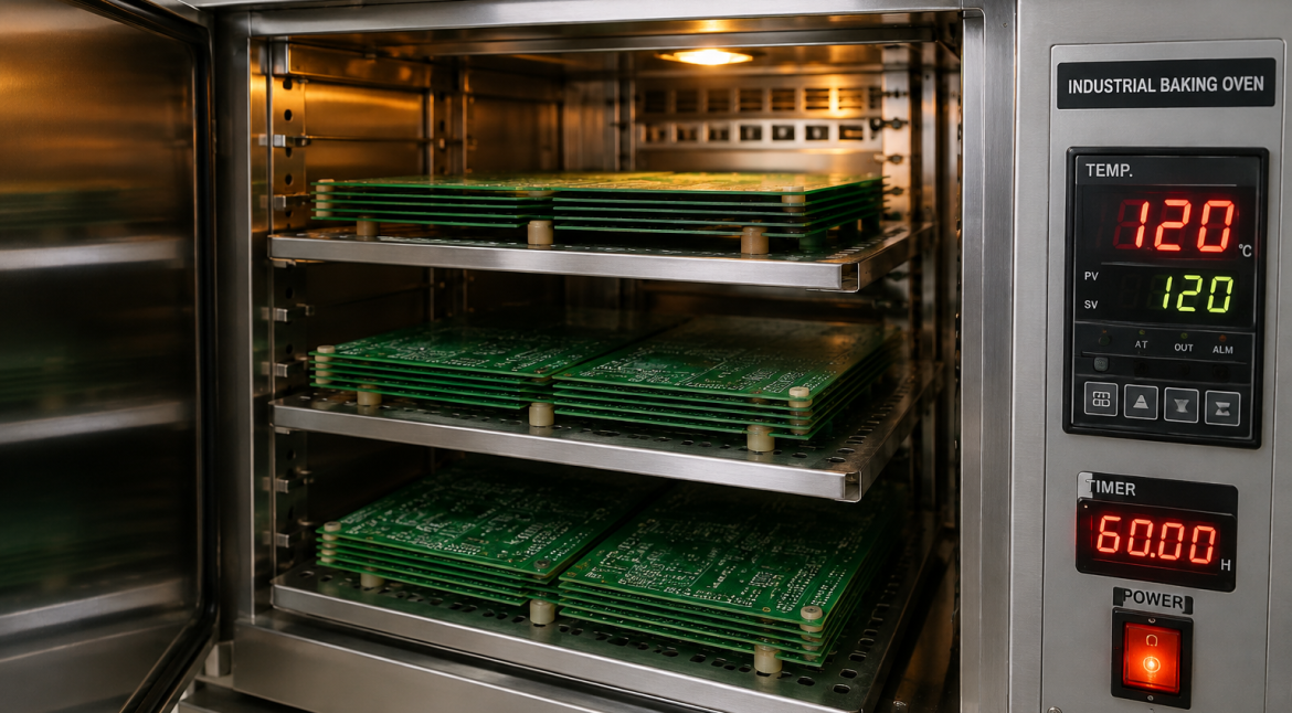
Reflow subjects the board to the highest temperature it will ever see, and it does so while the board is supported only at its edges on the conveyor. The combination of temperature and support position is what produces the classic bow at reflow.
Supporting the panel during reflow, running a profile with a controlled ramp and using a conveyor width that does not add constraint all reduce the risk. Where a board must be thin, the assembly fixture may need to hold it flat rather than relying on the panel stiffness. Poor support is also a common cause of placement defects, as described in SMT component shift causes.
Measurement
Warpage is measured by placing the board on a flat reference surface and measuring the maximum gap, or by scanning the surface with a height sensor. The reference matters: a board measured on a granite table will give a different figure from one measured on a production conveyor.
The measurement should be taken in a defined thermal state. A board measured cold and a board measured after reflow are different objects, and a specification that does not state the condition is not a specification. For assembled boards the measurement is usually taken at room temperature after reflow has cooled, since that is the state in which the board must fit its enclosure.
Consequences of Warpage
The immediate consequence is assembly yield. A warped board does not sit correctly against the stencil, so the paste deposit varies across the panel, and it may not sit correctly in the placement machine or the reflow fixture.
The longer term consequences are mechanical. A board that is bolted flat into a housing stores stress in the joints, which appear later as cracked solder fillets or lifted pads. Where the board carries a component whose position is critical, such as an optical sensor or a connector that mates with a housing, the warp becomes a functional error rather than a cosmetic one.
Design and Process Checklist
Balance the copper on both sides, keep the stackup symmetric, avoid mixing very different foil weights in the same build, and add stiffening rails to thin panels. Choose the laminate from the assembly temperature rather than only from the electrical requirement.
Specify the flatness limit and the condition under which it is measured, and verify it on a sample from the production run rather than on the first article alone. Where the design is at the limit, a small trial with a representative panel is worth more than any calculation, and it is far cheaper than discovering the problem after the full order has been assembled. The trial should use the production stackup, the production laminate and the production reflow profile, since those three variables are the ones that decide the result.
FAQ
Does warpage mean the board is defective? Not necessarily. Every board has some departure from flat; what matters is whether it is inside the limit for the assembly process and the final fit.
Can a warped board be flattened? A board can be pressed flat for measurement, but that stores stress rather than removing it. Heating a warped board above its glass transition temperature can relieve some distortion and can also create a new one.
Why does the board warp after assembly but not before? Because reflow takes it above the glass transition temperature, where the stored imbalance from lamination and the copper distribution can act. The same board cooled differently will distort differently.