PCB Holes Explained: Plated Through Hole, Via and Mounting Hole
A finished board is covered in holes of several different kinds, and confusing them is a common source of layout and manufacturing mistakes. Each type exists for one purpose, has its own plating requirement and its own set of rules. Knowing which is which makes a layout easier to check and a fabrication query easier to answer.
The Three Families
Holes on a board fall into three broad families. The first contains the holes that make electrical connections between layers, commonly called vias. The second contains the holes that hold a component in place, whether it is a screw or a through-hole part. The third contains the holes that exist only to help the manufacturing process, such as tooling and registration holes that align the panel through the drill and imaging steps.
The families overlap in appearance but not in requirement. A via that is expected to carry a supply current has to be plated and sized for that current; a mounting hole may be plated or not, depending on whether it is meant to connect to chassis ground; a tooling hole is defined by the fabrication process and is normally not a design decision at all.
Plated Through Hole Versus Non-Plated Hole
The distinction that matters most to the drill file is whether a hole is plated. A plated through hole has copper deposited on its wall, which connects the layers it passes through. A non-plated hole has no copper in it and connects nothing; it exists to accept a component lead, a screw or an alignment pin.
The two are produced by different process flows, and a hole that is accidentally specified as the wrong type produces a defect that cannot be corrected later. A non-plated hole that should have been plated leaves a net unconnected, which is a fault that only appears at electrical test. A plated mounting hole that was intended to be isolated can create an unintended connection between the board ground and the chassis.
What a Via Does
A via connects a signal on one layer to a signal on another. On a two-layer board it is a simple through hole connecting the two outer layers. On a multilayer board it may be a through via that passes through every layer, a blind via that reaches an inner layer from one surface, or a buried via that connects two inner layers without reaching either surface.
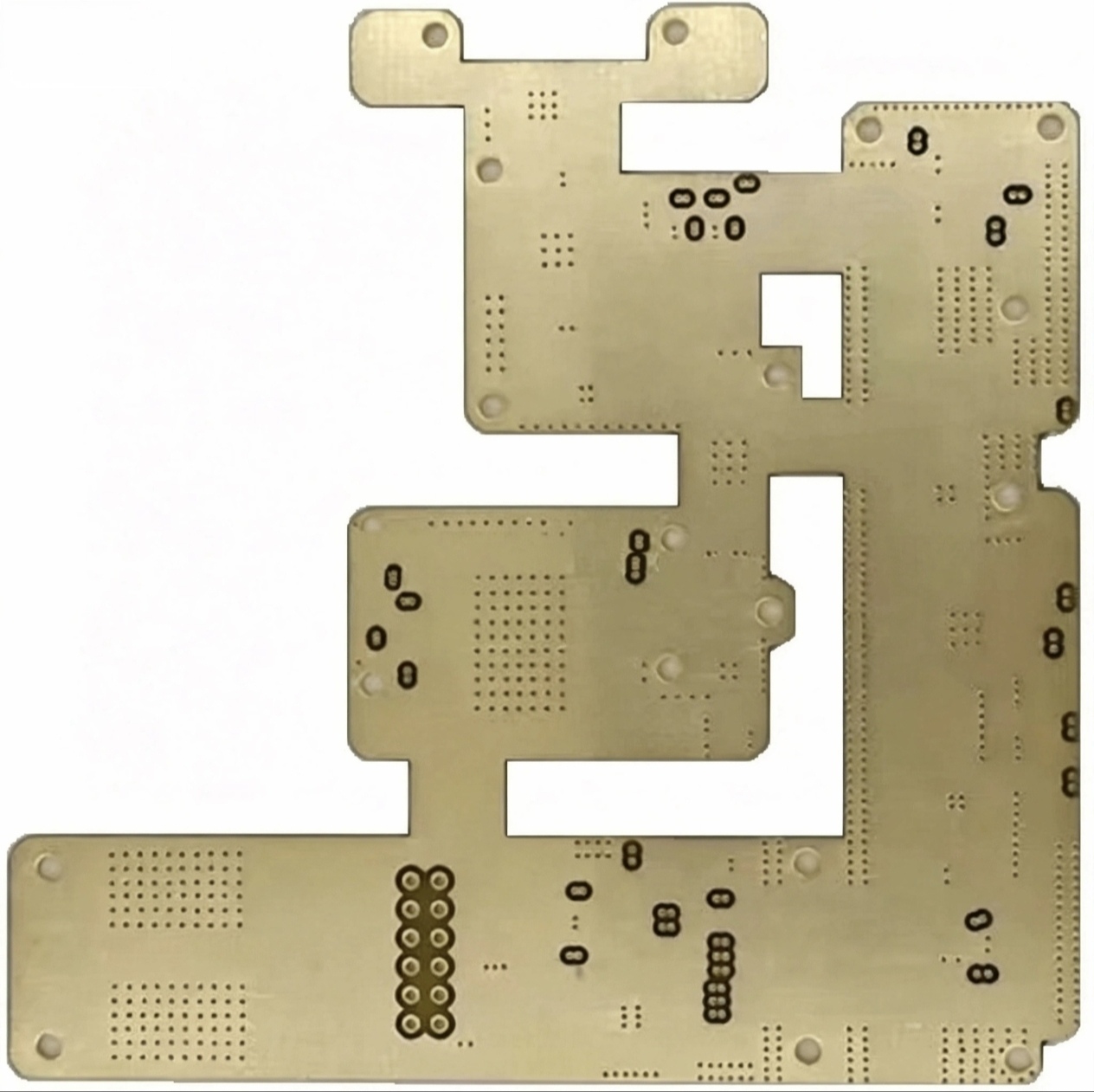
Vias also serve purposes beyond connection. A ground net that is kept unbroken on both outer layers of a two-layer board benefits from a large number of stitching vias, because they tie the two ground areas together and reduce the impedance between them. The same vias provide a degree of mechanical resistance to board flexing, and they reduce the parasitic capacitance that two large areas of copper form across the laminate. Our blind and buried via notes cover the more complex structures.
Via Size and Current
Via sizing follows the same logic as trace sizing. The barrel of a via has a cross-sectional area determined by its diameter and the plating thickness, and that area carries the current. A small signal via is adequate for a logic net, while a via carrying an ampère or more should be duplicated so that the current has several parallel paths. Where a high-current component connects to an internal plane, at least two vias to the plane is the common requirement.
The finished diameter of a plated hole is smaller than the drilled diameter by twice the plating thickness, and the fabricator’s capability determines the smallest reliable size for the panel thickness in use. Specifying a small via on a thick board raises the aspect ratio and makes uniform plating more difficult.
Component Holes and Insertion
A through-hole component needs a hole large enough to accept the lead and small enough to leave a solder fillet. The usual rule is to allow a clearance of around 0.2 to 0.3 millimetres over the nominal lead diameter, which accommodates the lead tolerance and the plating without leaving an oversized opening. A hole that is too large produces a joint with insufficient solder and poor mechanical strength, and it also increases the risk of solder wicking through to the other side.
Where a component body sits flat against the board, the drill size also sets the minimum pitch between adjacent holes. Dense through-hole connectors are normally specified with the manufacturer’s recommended hole pattern rather than being derived from the lead diameter, because the recommendation accounts for the insertion equipment as well as the solder joint.
Tooling, Registration and Mounting Holes
A tooling hole has no electrical function. It is used to align the panel or the board during drilling, imaging and assembly, and its position and diameter are dictated by the process. Registration holes serve a similar purpose during imaging, and their accuracy relative to the circuit pattern is what keeps the layers aligned. These holes are usually added by agreement with the fabricator rather than being placed by the designer.
A mounting hole is a design decision. If it is isolated from the electrical ground, it will accept a plastic standoff or an insulated screw. If it is connected to chassis ground, it provides a low-impedance path from the board to the enclosure, which is desirable for shielding but can be undesirable if the chassis is a noise source. The choice should be recorded on the drawing, because the difference between the two cases is invisible in the finished board.
Checking the Drill Specification
Before the design is released, confirm that every hole is specified as plated or non-plated as intended, that the hole sizes match the components being fitted, and that the via sizes are compatible with the panel thickness and the fabricator’s capability. A small number of holes specified incorrectly is enough to require a new tooling set, which costs more than the check would have. The design release checklist lists the drill checks, the hole copper material explains what the plating has to achieve, and the tooling hole notes describe how registration is handled in fabrication.
FAQ
Can a plated through hole be used as a mounting hole? It can, and it is often done deliberately to bond the board to a metal chassis. The consequences have to be accepted: the mounting point becomes part of the ground network, and a screw that works loose or a standoff that corrodes changes the electrical behaviour as well as the mechanical attachment. Where the connection has to be controlled, a defined component such as a zero-ohm resistor gives a deliberate link that can also be removed during diagnosis.
Why do some boards have so many small holes in the ground areas? They are stitching vias, and their purpose is to hold the ground areas on different layers at the same potential. A large number of them reduces the impedance between the layers, which improves noise performance and helps the board resist flexing. The spacing is chosen so that the two areas remain electrically close at the highest frequency of interest rather than being set by appearance.
What does gopcb check about holes before fabrication? We check the plated and non-plated classification of every hole against the design intent, the drill sizes against the components specified, and the via sizes against the panel thickness and our process capability. Most hole-related problems we see come from a drill file that was generated before a late change to the design, so we also confirm that the drill data matches the copper layers it is supposed to connect.