PCB Short Circuit Prevention: Design and Assembly Practices
A short circuit is the defect that wastes the most time in the assembly and bring-up phase, because it can damage parts before anyone notices it exists. Finding one after the fact is slow: the board may have hundreds of nets and only a few minutes of power-on time before a component fails. Preventing it is a matter of process discipline, and locating it quickly is a matter of designing the board so that the fault can be isolated. Both are part of PCB short circuit management.
The techniques below fall into two groups: what to verify during assembly, and what to design in so that a fault can be narrowed down to one area rather than to the whole board.
Assembly Practices That Prevent Faults
Hand soldering is where most avoidable shorts originate. Before any soldering begins, inspect the bare board visually and measure the resistance between each supply rail and ground. After each device is placed, repeat the supply-to-ground measurement. The interval is short, but it means a fault is attributed to the component that was just installed rather than to a board with twenty devices on it.
A second habit is controlling the iron. Flicking a hot iron to clear solder sends small spheres across the assembly, and a sphere resting between two fine-pitch leads is nearly impossible to see. Small surface-mount capacitors used for supply filtering are the most common victims, both because there are many of them and because their terminations are close together. Measuring the capacitors before installation, where the batch allows it, removes defective components from the list of possible causes.
Where a BGA package is involved, the risk changes character because the joints are hidden. Reflowing a large ball-grid array by hand is unreliable, and a bridge between an adjacent power and ground ball cannot be inspected optically. If rework is required, the board should be X-rayed afterwards rather than assumed to be good.
Locating a Short With the Layout Database
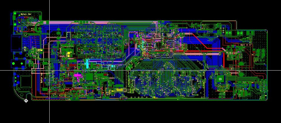
When a fault is confirmed, the layout file is the fastest diagnostic tool. Highlight the shorted net in the CAD viewer and look for where it runs closest to the other net, or where a plane edge, a via anti-pad, or a mask opening could allow a bridge. Two areas deserve a specific look: the smallest clearances in the design, and the interface between a plane and the pads connected to it.
The most common design-related cause is not a routing error but a process interaction. An solder bridge can form across a mask dam that is too narrow, or between pads on a component with a fine pitch, even when the copper spacing meets the drawing. In that case the mask geometry rather than the copper geometry is the thing to change.
Isolating the Fault by Cutting and Segmenting
On a two-layer board, cutting a trace with a knife is still an effective way to isolate a fault. Cutting the net into sections and testing each section separately narrows the search to a functional block, and the cut can be repaired afterwards with a wire link. The method is impractical on dense multilayer boards, where the relevant trace is buried.
For those boards, a dedicated short-circuit locator is the practical alternative. Instruments that inject a signal and trace the resulting field can identify the location of a low-resistance path across a plane without cutting anything. They are most useful when the resistance of the fault is low enough to be distinguished from the surrounding copper.
Whatever the method, the fault should be attributed to a root cause before the board is released. A short that is repaired without an explanation tends to reappear in the next build.
Designing the Power Distribution for Debuggability
The most valuable design measure is to segment the supply of each major device so that it can be disconnected independently. A ferrite bead or zero-ohm resistor in series with each device supply makes it possible to remove one load at a time and observe whether the fault disappears. On a board with several large digital devices, this single practice often reduces a day of debugging to a few minutes.
The segmentation should be present in the schematic from the start, because adding it later requires cutting traces. It also has an electrical benefit: the bead provides a degree of isolation between the supply of a noisy device and the rest of the rail.
Continuity and Insulation Testing
Every production board should pass a continuity check that covers the intended connections and an insulation resistance measurement that covers the nets that must remain separate. Bare-board electrical test does this at the fabrication stage before components are installed, which means a copper defect is detected while the board is still a blank panel and the cost of discarding it is low.
In-circuit test extends the same idea after assembly, measuring the resistance of each net against ground and against its neighbors. The limit for a pass is usually set well above the normal resistance of the net, so that a partially formed bridge with a few ohms of resistance is still detected rather than being accepted as a valid connection.
Process Control on the Fabrication Side
Not all shorts originate in assembly. Copper slivers left by etching, an incomplete etch between closely spaced traces, a plating nodule that bridges two conductors, and conductive debris trapped between layers all produce faults detected only at electrical test. These are controlled by etch process control, surface cleanliness before lamination, and inspection after etch.
The design contributes by avoiding geometries that sit at the limit of the process. Spacing at exactly the fabricator’s minimum, a mask dam at exactly the printable minimum, and a copper sliver-prone geometry all raise the probability of a bridge. Keeping a margin, where the area exists, costs nothing and removes a category of yield loss from the program. Related process considerations are covered in PCB design quality characteristics and in copper plating defect prevention.
Verification Before Power-Up
Before applying power to a first article, verify three things: the resistance from each rail to ground, the polarity of every polarized component, and the orientation of every device that has more than one valid orientation. Checking these on an unpowered board is quick, and it protects the parts that would otherwise be destroyed by a fault that takes longer to find than to prevent. First-article verification practices are described in multilayer PCB prototype requirements.
If a fault is found, the response should be systematic: confirm the fault, narrow it to a block, identify the mechanism, and only then repair the board. Repair without diagnosis produces a board whose reliability is unknown and a program that will see the same defect again. Assembly-side causes of unexpected faults are discussed in SMT component shift causes.
FAQ
Can a short circuit be caused by the laminate itself? Yes, though it is less common than assembly faults. Conductive anodic filament growth between closely spaced conductors under humidity and bias, plating nodules that bridge a gap, and conductive debris laminated into the stack all produce shorts that appear only after assembly or after some time in the field.
Is cutting a trace an acceptable repair? For a prototype it is a legitimate debugging step, and a repaired cut with a wire link is acceptable if the link is short, secured, and does not disturb the impedance of a critical net. For production it is not a repair method, because the change cannot be documented or repeated reliably.
How do I make a large board easier to debug? Segment the supply of each functional block with a ferrite bead or a zero-ohm link, provide test access to every rail, and keep the ability to isolate a block without cutting copper. The design cost is small and the debugging benefit is immediate.