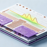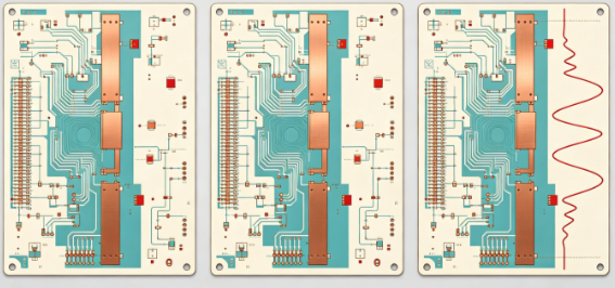
In high-speed multilayer PCB manufacturing, engineers often focus on trace width, copper thickness, dielectric constant, and etching compensation when controlling impedance. However, PCB thickness tolerance can also have a significant influence on impedance consistency because changes in the pressed dielectric structure directly affect the distance between signal traces and their reference planes.
A PCB may pass initial impedance calculations but still show unexpected TDR variations across different areas of the same panel. When this happens, the problem may not necessarily be an inaccurate simulation model. Local variations in dielectric thickness, resin distribution, copper thickness, and pressing conditions can change the actual transmission-line geometry.
For high-speed designs, PCB thickness tolerance should therefore be considered together with stackup construction and impedance control rather than treated only as a mechanical dimension.
How PCB Thickness Variation Affects Impedance
For a microstrip or stripline structure, characteristic impedance is determined by the relationship between trace geometry and the surrounding dielectric structure.
A simplified relationship can be expressed conceptually as:
[Z_0=f(W,T,H,D_k)]
where:
- (W) = trace width
- (T) = copper thickness
- (H) = distance between the signal trace and reference plane
- (D_k) = effective dielectric constant
The exact impedance relationship depends on the transmission-line geometry, so a simple proportional formula should not be applied universally.
Among these parameters, dielectric thickness (H) is particularly important. If the distance between the signal trace and reference plane changes while trace width remains unchanged, the electric-field distribution also changes.
For a typical multilayer PCB, this distance is strongly influenced by the pressed prepreg structure.
Therefore, a variation in finished board thickness does not automatically equal the same percentage variation in impedance. Instead, it is an indicator that the internal dielectric geometry may have changed and should be investigated.
Why the Pressing Process Creates Local Dielectric Variation
In a multilayer PCB, the nominal thickness of a prepreg sheet is not necessarily the final dielectric thickness after lamination.
During pressing, resin flows into the spaces between copper features and is compressed under temperature and pressure. The final dielectric thickness depends on several interacting factors, including:
- Prepreg resin content
- Glass-weave construction
- Copper pattern density
- Copper thickness
- Resin flow behavior
- Pressing pressure
- Temperature profile
- Heating and cooling rate
- Lamination cycle
- Panel size and construction
This means the center and edge regions of a panel can experience different mechanical and thermal conditions.
Copper distribution can also influence local resin flow. A region with large copper planes may behave differently from an area with sparse traces. As a result, the actual dielectric thickness may vary spatially even when the same prepreg material is used across the entire stackup.
For high-speed multilayer PCB designs, this local variation can become part of the impedance-control problem.
PCB Thickness Tolerance Can Reveal Internal Stackup Variation
Finished board thickness is not the same as dielectric thickness.
A board may become thicker or thinner because of changes in:
- Copper thickness
- Resin content
- Glass fabric
- Prepreg compression
- Inner-layer copper pattern
- Outer-layer plating
- Surface finish
Consequently, measuring only finished board thickness cannot directly determine the impedance of a transmission line.
However, abnormal board-thickness distribution can provide an important manufacturing signal.
For example, if TDR measurements show that impedance changes consistently across the same physical region where board thickness also varies, engineers should investigate whether the pressed dielectric thickness has changed.
This correlation is much more useful than assuming that the board-thickness measurement alone proves the cause of impedance variation.
The Relationship Between Dielectric Thickness and Dk
Another important factor is the effective dielectric constant.
The dielectric environment around a high-speed trace is determined not only by the nominal material data sheet value but also by the actual resin/glass distribution and transmission-line geometry.
Prepreg contains glass reinforcement and resin. After lamination, the local resin content and glass-weave position can affect the effective dielectric environment seen by the signal.
Therefore, two regions made from the same prepreg material can have slightly different effective electrical properties.
This is particularly important when the dielectric thickness changes at the same time.
For example:
Dielectric thickness changes → field distribution changes → effective impedance changes
At the same time:
Glass/resin distribution changes → effective Dk changes → impedance changes
When both effects occur together, the resulting impedance variation can be larger than expected from a mechanical thickness measurement alone.
Why Nominal Prepreg Thickness Is Not Enough
Using the nominal thickness of a 106, 1080, 2116, or 7628 prepreg sheet directly in a high-speed impedance model can introduce errors if the actual pressed thickness differs significantly from the design assumption.
The final stackup should be based on the manufacturer’s validated lamination data whenever possible.
Important information includes:
- Pressed dielectric thickness
- Resin content
- Copper weight
- Copper pattern distribution
- Finished board thickness
- Lamination tolerance
- Effective Dk
- Df
- Impedance coupon results
For demanding impedance control applications, the PCB manufacturer and designer should agree on the stackup before production rather than allowing the fabrication process to determine the final dielectric geometry without electrical verification.
Why Copper Thickness Also Matters
Engineers sometimes attribute impedance variation entirely to board thickness, while overlooking copper thickness.
Copper thickness affects both the physical dimensions of the transmission line and its conductor loss.
For a high-speed trace, the actual copper profile after etching and plating can differ from the nominal copper weight.
Important variables include:
- Starting copper foil thickness
- Etching reduction
- Plating thickness
- Trace sidewall profile
- Copper roughness
- Surface treatment
- Inner- and outer-layer copper differences
For this reason, an accurate impedance model should use realistic copper dimensions whenever process capability data are available.
Three Practical Controls for Impedance Consistency
1. Control the Lamination Stackup
The first step is to establish a realistic pressed stackup.
Instead of using only nominal prepreg thickness, engineers should obtain validated pressed-thickness data from the PCB manufacturer.
The stackup should specify:
- Layer sequence
- Copper thickness
- Prepreg type
- Core thickness
- Target dielectric thickness
- Target impedance
- Manufacturing tolerance
For complex high-speed boards, stackup simulation should include realistic manufacturing tolerances rather than a single ideal value.
2. Correlate Thickness Measurements With TDR Data
A useful quality-control approach is to compare physical thickness data with impedance measurements from the same production lot.
For example:
- Measure board thickness at multiple locations.
- Measure impedance on corresponding test coupons.
- Map the physical location of impedance deviations.
- Compare the data with copper thickness and lamination records.
- Determine whether the variation is systematic or random.
A three-point or multi-point board-thickness measurement is generally more informative than relying on a single measurement location.
However, the number and location of measurement points should be defined according to board size, customer requirements, and the applicable manufacturing specification.
3. Include Manufacturing Tolerances in the Impedance Model
An ideal stackup simulation may produce a precise 50 Ω result, but production cannot reproduce every dimension exactly.
A practical PCB design workflow should therefore evaluate impedance sensitivity to:
- Dielectric thickness
- Trace width
- Copper thickness
- Dk variation
- Etching tolerance
- Registration tolerance
- Surface copper/plating
Sensitivity analysis can identify which variable contributes most strongly to the impedance variation.
This allows engineers to focus process-control resources on the parameters that have the greatest electrical impact.
Why Board Thickness Alone Cannot Be Used to Predict Impedance
A common engineering mistake is to assume:
Board thickness increases → impedance increases.
The actual relationship is more complicated.
For example, if the finished board becomes thicker because of additional copper plating on the outer layers, the internal signal-to-plane dielectric thickness may remain almost unchanged.
In contrast, if board thickness changes because the prepreg has different compression behavior, the internal dielectric spacing may change significantly.
Therefore, PCB thickness tolerance should be treated as a manufacturing indicator rather than a direct impedance equation.
The correct analysis is to determine which physical layer or material parameter caused the finished thickness variation.
High-Speed Applications Require More Detailed Verification
For high-speed digital designs, impedance variation can contribute to:
- Increased reflections
- Higher return loss
- Insertion-loss variation
- Timing uncertainty
- Inter-symbol interference
- Eye-diagram degradation
- Differential-mode imbalance
The severity depends on signal rise time, channel length, operating frequency, impedance tolerance, and receiver sensitivity.
A low-speed PCB may tolerate relatively large dimensional variation without a noticeable electrical impact, while a high-speed interface can be much more sensitive to small changes in transmission-line geometry.
Therefore, signal integrity analysis should be based on the actual channel requirements rather than applying one universal board-thickness limit to every application.
TDR Is Useful, but It Should Be Used Correctly
Time-domain reflectometry is an effective method for locating impedance discontinuities along a transmission path.
If the TDR waveform shows a repeatable impedance shift in a particular section, engineers can correlate that position with:
- Stackup transitions
- Copper-density changes
- Via fields
- Connector transitions
- Lamination structures
- Reference-plane changes
However, TDR does not directly identify the root cause.
A TDR result should be combined with cross-sectional analysis, dimensional measurements, stackup information, and manufacturing records.
For differential interfaces, differential impedance should also be evaluated separately from single-ended impedance.
Common Mistakes in PCB Thickness and Impedance Control
Several mistakes can make high-speed impedance troubleshooting unnecessarily difficult.
Mistake 1: Using nominal stackup data as production reality
Simulation should use the manufacturer’s validated construction data whenever possible.
Mistake 2: Measuring finished board thickness at only one point
Local lamination variation can be missed by single-point measurement.
Mistake 3: Treating board thickness as dielectric thickness
Finished board thickness includes copper, dielectric, and surface-finish contributions. It does not directly represent the signal-to-reference-plane distance.
Mistake 4: Ignoring copper pattern distribution
Different copper densities can influence resin flow and final dielectric thickness.
Mistake 5: Adjusting trace width before investigating stackup variation
Changing trace width may compensate for one region while making another region worse. Root-cause analysis should come first.
Recommended Checklist for High-Speed PCB Projects
Before releasing a high-speed PCB design, engineers can verify the following:
- Confirm the actual pressed stackup with the manufacturer.
- Define target dielectric thickness for critical impedance layers.
- Include copper thickness and plating in the impedance calculation.
- Review prepreg resin content and glass-weave construction.
- Evaluate lamination tolerance.
- Measure finished board thickness at multiple locations.
- Correlate physical measurements with TDR impedance results.
- Use realistic Dk values and manufacturing tolerances.
- Verify differential and single-ended impedance independently.
- Perform cross-sectional analysis when significant deviations occur.
- Review the complete channel when impedance variation affects system performance.
How Kingda Supports Impedance-Controlled PCB Manufacturing
Consistent impedance control requires close coordination between PCB design, stackup engineering, lamination, copper processing, and electrical testing.
Kingda can support high-speed multilayer PCB projects by coordinating stackup design, material selection, lamination control, copper processing, impedance coupons, and production verification.
By incorporating actual manufacturing tolerances into the design and correlating physical dimensions with electrical measurements, engineers can reduce unexpected impedance variation and improve consistency from prototype builds to mass production.
Conclusion
PCB thickness tolerance can influence impedance consistency when it reflects changes in the internal dielectric structure of a multilayer board.
The key variable is not simply the total finished board thickness. What matters electrically is the actual relationship between the signal conductor, reference plane, copper geometry, and dielectric environment.
For high-speed applications, reliable impedance control therefore requires more than an ideal stackup calculation. Engineers should combine realistic pressed-thickness data, copper dimensions, effective dielectric properties, manufacturing tolerances, TDR measurements, and cross-sectional analysis.
When physical stackup data and electrical test results are correlated throughout production, PCB manufacturers and designers can identify the real source of impedance variation and establish a more stable manufacturing process.