AI Accelerator PCB: Why Training and Inference Diverge
At its Cloud Next event in April 2026, Google announced its eighth generation tensor processing units and, for the first time, split a single generation into two systems with different purposes. One is aimed at large scale pretraining and scales to 9,600 chips in a superpod with two petabytes of shared high bandwidth memory. The other targets inference and reinforcement learning, connecting 1,152 chips in a pod through a different network topology. The company reported up to 2.7 times better training price performance and an eighty percent improvement on inference, which means an AI accelerator PCB now has to serve two rather than one set of design goals.
For an AI accelerator PCB the split matters more than any single specification. Training and inference place different demands on interconnect, bandwidth, power and therefore on the board, and designs that were previously similar are becoming distinct products with their own rules. Understanding which one a programme is building determines the stack up, the material and the manufacturing partner.
One Generation, Two Architectures
Training systems optimise throughput across a very large number of chips. That means enormous aggregate bandwidth between accelerators, a network topology that tolerates long distances, and power delivery capable of feeding racks that draw hundreds of kilowatts. Board area is dominated by interconnect and power rather than by logic.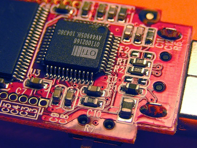
Inference systems optimise latency and efficiency for a single request or a batch of requests. They benefit from large on chip memory, shorter network diameters and a topology designed to keep communication local. The board carries more density per unit area and shorter, faster links rather than the longest reach.
What Training Boards Carry
A training board concentrates accelerator packages, high bandwidth memory interfaces and a very large number of high speed differential channels. Layer counts are high because each channel needs a reference plane and because power planes must be large enough to deliver current with low impedance.
Materials are chosen for the lowest loss the budget allows, and copper weight rises to carry current. In the most demanding designs, additional board types such as midplanes and switch boards appear inside a single rack, each with its own layer structure and its own manufacturing difficulty.
What Inference Boards Carry
Inference hardware pushes density instead. Packages are placed closer together, the escape routing from each package consumes layers quickly, and the demand for short connections favours microvia structures that allow direct vertical paths through the stack.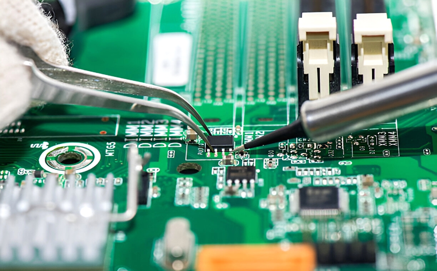
Because inference boards are often produced in larger quantities than training systems, cost control matters more. That produces a different design philosophy: the highest grade material only where the channel length requires it, a stack up optimised for manufacturability, and a layout that keeps the process inside the factory’s comfortable window rather than at its limit.
Optical Interconnect Moves Onto the Board
As electrical channels reach their practical reach, optical links take over the longest connections. That places optical module cages and their high speed host interfaces on the board, together with the power and thermal infrastructure they require. The result is a board that mixes very high speed electrical routing with optical interfaces and their mechanical constraints.
Design implications are significant. Module locations are fixed by faceplate geometry, so high speed channels must be routed to defined positions, and the loss budget for each channel has to be tracked from the package to the module. Where these links carry the accelerator interconnect, a channel that misses its loss target affects system performance rather than a single port, which raises the importance of impedance and loss control in fabrication.
Topology Choices Become Board Decisions
Network topology determines how many connections leave each package and how long they are. A three dimensional torus spreads connections in all directions, which on a board translates into many channels of moderate length. A flatter topology with a smaller network diameter reduces hop count and latency but concentrates more connections in a smaller area.
Each choice changes the routing problem. Concentrated topologies demand higher density and more layer transitions, while distributed topologies demand longer channels with tighter loss budgets. Since the topology is fixed by the system architecture, the board designer inherits the constraint and must make the stack up support it.
Package Escape and Memory Interfaces
Contemporary accelerator packages have thousands of connections, and routing them off the package is often the densest part of the design. Microvias placed under the package allow escape without consuming the surface, and they also allow decoupling capacitors to sit directly beneath the die where they are most effective.
Memory interfaces add another constraint because they are wide, fast and sensitive to length matching. On packages with high bandwidth memory, hundreds of parallel signals must reach the package with matched delays and consistent impedance, so the memory region of the board is usually designed first and the rest of the layout works around it.
Power Delivery at Accelerator Scale
An accelerator package can draw several hundred amperes at low voltage, and the power network must supply that with minimal drop and minimal inductance. Thick copper, wide planes and short vertical connections through microvias are all used together, and in some designs copper is embedded in the board to provide cross section without adding layers.
Thermal behaviour is coupled to the same structure, because the copper that carries current also carries heat. Design teams model the two together, and manufacturing has to deliver consistent copper thickness and dielectric spacing so that the modelled behaviour matches the built board. That requirement is one reason controlled fabrication processes are essential for accelerator products.
Thermal Load in a Dense Rack
Racks built for training draw power at a level that makes thermal design an architecture problem rather than a component choice. Boards operate in a warm environment and must not lose electrical performance as they heat, which puts the emphasis on material stability over the operating range rather than on room temperature measurements.
Mechanically, heavy heatsinks and cold plates load the board and the socket, so warpage control and flatness matter for reliable assembly. On thick boards with high copper content, achieving that flatness requires balanced copper distribution and controlled lamination rather than additional mechanical correction afterwards.
What Is Public and What Is Not
Industry discussion of accelerator boards frequently cites specific layer counts and module counts that have not been confirmed by the developer. Numbers circulated for one generation are often applied to the next without evidence, and the figures describing a 44 layer board with eighteen optical modules have been associated in public material more closely with the previous generation than with the newest one.
For anyone planning a programme, that distinction matters commercially. Designing to a specification taken from an unverified report produces an expensive board with margins that may not be needed, while designing to a validated channel budget produces the same performance for less cost. Verifying requirements with the actual system designer remains the only reliable route.
Qualifying a Board for an Accelerator Programme
Qualification for this class of product concentrates on channel performance and consistency. Impedance and insertion loss measurements on coupons, verification of registration across a large panel, and evidence that the process holds on repeated builds are the substance of the evaluation, and they take longer than a typical prototype cycle.
Buyers should also ask how the factory handles back drilling where stubs matter, how it controls plating in high aspect ratio holes, and what yield it has achieved on comparable structures. Those answers reveal whether a supplier is prepared for a programme whose value per rack is now measured in tens of thousands of dollars, and they are more useful than a capability list.
Material Choice Per Layer
Accelerator boards rarely use one laminate throughout. The layers carrying the fastest channels get the lowest loss material, while power and control layers use a less expensive grade. That decision reduces cost but creates a mixed stack whose behaviour depends on how the materials interact during lamination.
Different materials expand at different rates, so a mixed stack requires compensation in the artwork and careful process parameters. Designers who choose materials per layer rather than per board should confirm the combination with the manufacturer before release, because that is where an apparently economical stack up turns into a yield problem. It is a stack up decision as much as a purchasing one, and it belongs in the layout and stack up review.
Testing Channels Before Rack Integration
A board carrying accelerator interconnect is expensive to install and very expensive to replace once a rack is built. Testing therefore has to verify channel behaviour before integration, which means measuring insertion loss and impedance on representative channels as well as checking continuity.
The practical approach combines coupon data from production with a sample of channel measurements on the assembled board. When a threshold is crossed, the data shows whether the cause is a board process excursion or an assembly effect, and it allows a decision to be made before the unit enters a system. Building that capability into assembly testing is far cheaper than discovering the problem in the data centre.
Where This Leaves Designers
The divergence between training and inference hardware means there is no single best accelerator board. Training rewards bandwidth, power and the lowest achievable loss; inference rewards density, latency and cost discipline. A design that ignores which of those it is optimising will spend money in the wrong place.
Practically, that means defining the channel budget and the thermal envelope early, choosing materials per layer rather than per board, and working with a manufacturer who can build the resulting mixed structure consistently. Suppliers who can discuss the whole manufacturing route from stack up to test are the ones able to support both variants of a platform without relearning the process each time it changes.