AI Glasses PCB: Fitting an Agent Into a Temple Arm
AI glasses PCB design changed character on 2 September 2026, when Tencent opened its WorkBuddy platform to more than a hundred ecosystem partners and launched a co-branded pair of AI glasses with Rokid, while Alibaba released a glasses edition of its Qoder tool on the same hardware. Both products run the glasses as a first person sensor and the cloud agent as the reasoning layer, which turns a device built for occasional capture and translation into a terminal for meeting notes, enterprise search, data preparation and on site recognition.
That change reaches the board before it reaches the software, because continuous use means the camera, microphone array, wireless link and controller have to run longer while exchanging data with a phone, a computer and a remote agent. The temple arm does not grow to accommodate that workload, so the printed circuit has to absorb it inside the same enclosure volume.
What Changed When Glasses Joined a Workflow
Consumer smart glasses spend most of their time idle. A device that joins an office workflow spends much of its time sensing. Microphones stay open for transcription, the camera is triggered frequently, the wireless link maintains a session with a host device, and the processor runs speech and vision models or streams to the cloud when latency matters.
The electronics consequence is not a higher component count alone. It is that power, thermal and reliability margins shrink because the duty cycle rises. Components that were specified for intermittent operation now run continuously, and the heat they generate has nowhere to go inside an injection moulded temple arm with no fan and limited surface area.
The Temple Arm Sets the Envelope
A pair of glasses is a mechanical product before it is an electronic one. Weight distribution decides whether the device is comfortable, and the temple arm is the least forgiving place to add mass because it sits behind the ear. Every board decision therefore has an owner in the mechanical design, and the answer to a routing problem cannot be a thicker stack.
The usable volume is a narrow beam with a curved profile that must clear the hinge, the battery and the antenna region. Radio frequency performance adds a further constraint, because antennas need clearance from copper, and a ground plane placed for electrical convenience can detune an antenna that was carefully matched. Layout for this product is a negotiation between mechanical, radio and thermal requirements, and it usually converges on a small number of rigid boards joined by flexible sections rather than on one large board.
Micro HDI Where the Processor Sits
Around the main processor the net count is highest: memory, power management, wireless, camera interface and audio all converge in a few square centimetres. Microvia HDI is used there because laser drilled vias and finer lines allow a high pin count package to fan out without consuming the whole board in escape routing.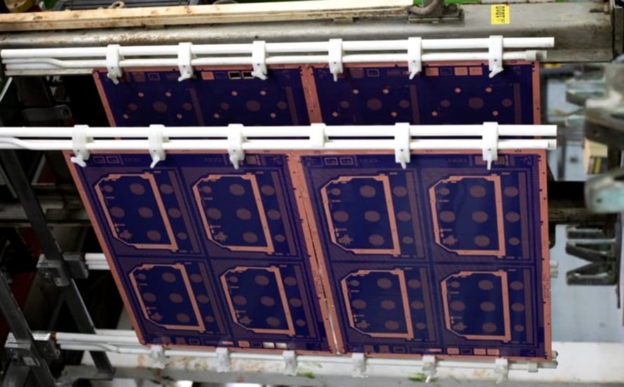
The manufacturing difficulty is concentrated in the same place. Fine line widths are more sensitive to exposure and development variation, small microvias demand precise laser drilling and void free plating fill, and several build up layers multiply registration requirements. A board like this is judged by whether those steps hold simultaneously across a batch, which is a different question from whether a single panel can be produced. Factories building this class of work usually describe it as a microvia HDI capability, and the evaluation should focus on process data rather than on the finest line ever demonstrated.
FPC and Rigid-Flex Through the Hinge
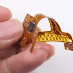
The hinge is the second concentration of engineering effort. It moves thousands of times, it is the narrowest part of the assembly, and it is where a conventional connector and cable would consume space that does not exist. Flexible circuits route the signals across it, and rigid flex constructions combine the stiff control area with a thin tail that crosses the joint.
Design rules that apply to any dynamic flex application apply here with less margin: conductors should run parallel to the bend rather than across it, the coverlay opening has to be positioned so the bend occurs in the flexible region, and stiffeners control where bending is allowed to start. Fatigue life then depends on bend radius and on how the mechanical assembly constrains the movement. Because those decisions are fixed by tooling, they need to be settled with the flex manufacturer before the first article is ordered, and a supplier experienced in flexible circuit assembly is usually involved at the layout stage rather than at the purchase order.
Signal Integrity on a Very Small Board
Camera interfaces and high speed links between the processor and memory behave like any differential channel: they need controlled impedance, a continuous reference plane and a return path that follows the signal. On a small board those conditions are harder to preserve because the layout is congested and layer transitions are frequent.
The practical discipline is to plan the stack up before routing begins, to reserve layers for high speed signals and keep power and ground references continuous beneath them, and to treat every via transition as a discontinuity that must be matched across the pair. Audio is the other sensitive region, because microphone inputs are low level and sit close to switching regulators and to a radio that transmits in bursts. Separating those domains in the stack up costs nothing at design time and a great deal if it is attempted after the layout is complete.
Thermal and Power Budget in Continuous Use
Heat in a wearable cannot be removed by a fan and there is little metal to spread it. The board itself becomes part of the thermal path, and copper area, thermal vias and the placement of the hottest components relative to the enclosure are all part of the design rather than an afterthought.
The power budget interacts with this directly. Continuous sensing increases average current, which raises temperature, which increases leakage and degrades battery life, so the design has to be efficient rather than merely capable. Practically, that means regulators placed close to their loads, short high current paths, and a charging path that can handle the current without generating local hot spots under the pad. Temperature rise measured on a finished assembly, not calculated from a datasheet, is the figure that matters.
Assembly: Small Parts, Narrow Process Windows
Micro boards use the smallest passive components, fine pitch packages and connectors with contact spacing measured in fractions of a millimetre. The process window for solder paste printing narrows accordingly, because the paste volume that produces a reliable joint on one small pad produces a bridge or an open on the next. Placement accuracy and reflow profile tolerance tighten at the same time.
Component placement also becomes a mechanical problem. Cameras must be aligned to the optical axis, microphones need acoustic ports clear of obstructions and adhesive, and connectors have to survive repeated mating during test and assembly. Designing those features with the assembly process in mind is what keeps a wearable product buildable, and it is the reason a defined assembly process should be part of the early design discussion.
Inspection and Test for Micro Assemblies
Inspection is not optional at this scale. Solder paste inspection verifies volume and position before reflow, automated optical inspection finds placement and soldering defects afterwards, and X-ray is needed for joints hidden under packages and for the fill quality of microvias in the board itself. Functional testing then exercises the camera, audio and radio paths together, because those subsystems only reveal interference problems when they operate simultaneously.
The value of testing early is diagnostic rather than statistical. When a radio link drops under load or a microphone shows noise, the cause could sit in the board, the assembly or the mechanical integration, and a test sequence that isolates the stages shortens the investigation considerably. Keeping assembly testing with the same supplier that builds the board makes that isolation straightforward.
Why Board and Assembly Should Share One Chain
AI glasses iterate quickly. Camera modules change, the processor platform is updated, and the enclosure is revised as the product finds its use case. Each of those changes can alter the board stack up, the placement of components or the flex routing, and if fabrication, assembly and test sit with different suppliers, every revision becomes a coordination exercise.
Working through one chain keeps the stack up, the stencil, the placement program and the test coverage aligned, so a change is evaluated once rather than negotiated three times. For a product that is still defining what it does, that responsiveness matters more than the last few percent of unit cost, and it is usually what determines whether a development schedule holds.
What the Next Stage Rewards
Tencent and Alibaba extending agent capability to glasses does not by itself create a mass market. It does, however, change what the hardware has to do, and that change favours manufacturers who can produce dense, thin, reliable assemblies rather than those who simply own capacity.
The competitive unit becomes manufacturing capability per unit volume: how much routing density can be placed in a temple arm, how reliably the assembly survives continuous use, and how quickly the design can adapt when the software platform moves. Suppliers who can answer those questions with process data and with a demonstrable fabrication flow will be the ones asked to build the next generation.