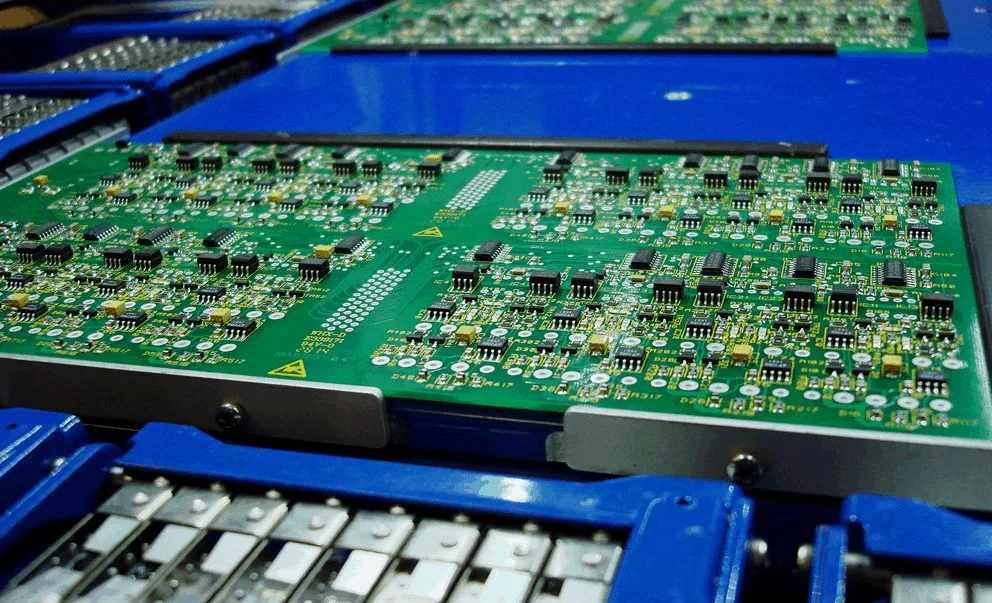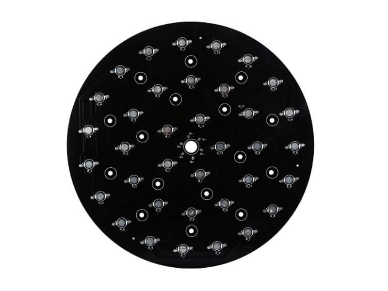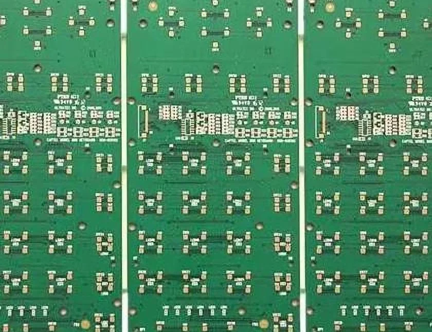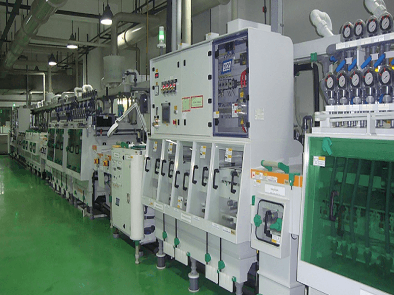
Plating Bath Agitation: 5 Methods for Even Copper Deposition Plating bath agitation does the work that chemistry alone cannot. Copper ions reach the panel surface through a thin layer of stagnant solution called the boundary layer, and that layer is where deposition slows down and thickness spread begins. Move the…

Tooling Plate Maintenance: 6 Steps for Flat PCB Lamination Tooling plate maintenance rarely gets attention until boards come out of the press with thickness variation, resin starvation or shifted inner layers. By then the cause is usually a plate that has been dented, warped or loaded with cured resin for…
Cooling Rate After Reflow: What It Sets in the Joint The cooling segment is the part of a reflow profile that most shops never specify. The ramp, the soak and the peak are tuned and recorded, and then the board is allowed to cool at whatever the last few zones…
X-ray Oblique Views: Seeing What a Top-Down Scan Misses X-ray inspection produces a shadow, and a shadow of a ball grid array taken from directly above hides a great deal. The balls overlap, the package substrate masks the top of each joint and a joint that has lifted from its…
Hot Air Leveling Flux Control: 6 Variables for Even HASL Coating Hot air leveling remains one of the most demanding steps in a PCB shop, and the hot air leveling flux often decides whether a panel leaves the machine with an even coating or a patchy one. Flux does three…
Stencil Foil Thickness Selection: Area Ratio and Paste Volume The stencil foil thickness sets the volume of solder paste that a single print can deliver, because the aperture in the foil is a small reservoir of fixed depth. Choose a foil that is too thin and fine-pitch parts get enough…
Plating Hull Cell Test: Reading Bath Balance Before Production A hull cell test plates a small panel across a wide range of current density in one step, and the pattern it leaves shows the state of the plating bath. It is the quickest way to see whether an additive is…
Component Placement Offset: Fiducial Recognition and Vision Alignment A placement offset is the difference between where a component sits and where the pad pattern says it should sit. Small offsets are absorbed by the self-aligning action of the solder during reflow; larger ones leave joints with unequal fillets, reduce the…
Black Hole Direct Plating: Carbon Process Control for Hole Walls Black hole direct plating makes a drilled hole conductive with a carbon dispersion instead of a copper layer, so the panel goes into the plating line without a chemical copper step. It removes a complex and expensive process, and in…
PCB Test Point Design: 7 Rules for Reliable ICT Access A PCB test point design decides whether the assembly can be probed at all, and it is a small piece of layout work with a large effect on test cost. A board that cannot be reached needs a fixture change,…