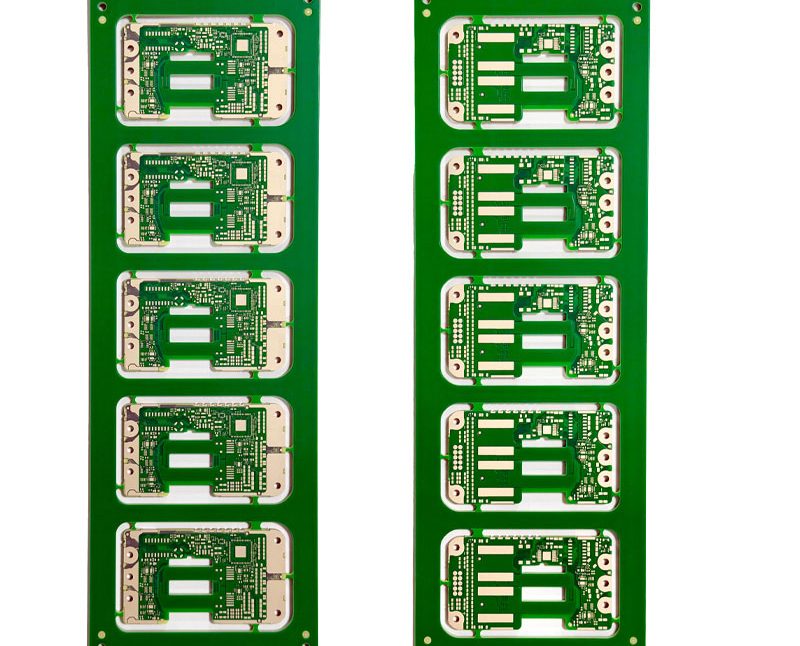
PCB Routing vs V-Scoring vs Die Cutting: Choosing a Profile Method Every board leaves the factory inside a panel, and the way it is separated from that panel determines the edge quality, the tooling cost and how much stress the components see. The three production methods in common use are…
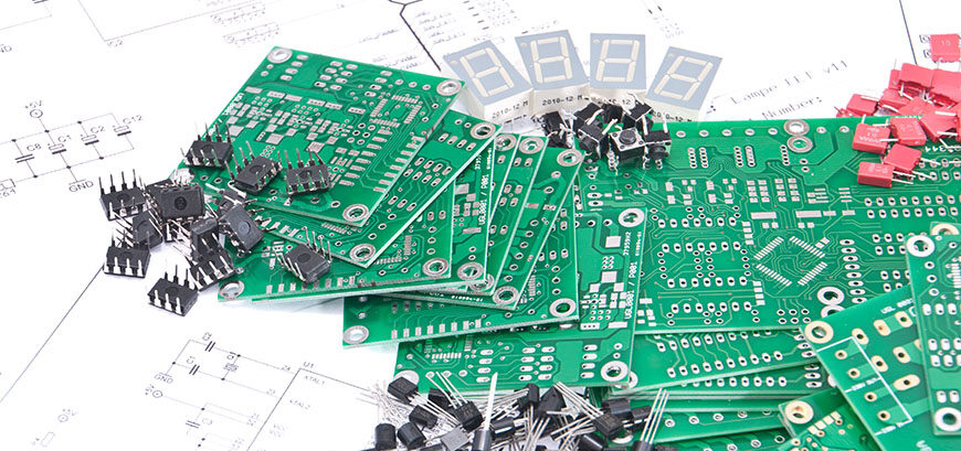
Six-Layer PCB Design Rules and Stack Choices A six-layer board is the point at which a design stops being constrained and starts being comfortable. Four layers give a ground plane and a power plane, but only two signal layers to route on, and those two layers are often in conflict…
High Frequency PCB: From Prototype to Production A high frequency board rarely goes straight from a sketch to a production line. It is designed once to prove the concept, then redesigned to be manufacturable, then optimised until the loss and the impedance tolerance meet the specification, and only then released.…
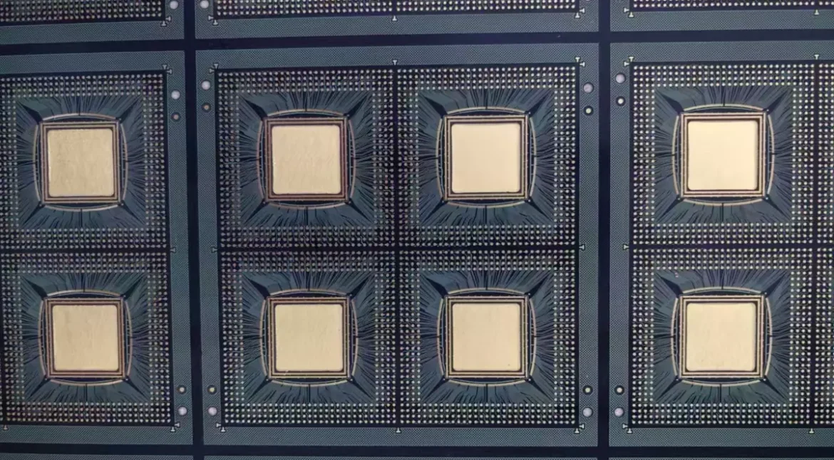
Aluminium Nitride Ceramic Substrate: Properties and Uses When a circuit has to run hot and be electrically isolated at the same time, the substrate stops being a passive carrier and becomes a thermal component. Aluminium nitride is a ceramic that conducts heat like a metal while remaining an electrical insulator,…
Military Grade PCB vs Industrial Grade: Key Differences The difference between a military grade PCB and an industrial grade PCB is not a single specification but a whole approach to margin. Both may be built on similar laminates and both may carry similar components, but the military version is designed,…
Four-Layer PCB Stack Arrangements and Trade-Offs A four-layer board is the point at which a printed circuit stops being a wiring carrier and starts being a controlled electrical environment. Adding two inner layers gives the designer a ground plane and a power plane, and those two elements change the behaviour…
Metallized PCB Edge: Edge Plating and Castellation Design A metallized PCB edge carries copper onto the side wall of the board, either as a continuous plated band or as a row of castellated half holes. The first is used mainly for shielding, grounding and current return; the second turns a…
Moisture Sensitive Devices: PCB Design and Handling Rules Plastic packages absorb water from the air. When an assembled board enters a reflow oven, that water turns to steam inside the package and the pressure has to go somewhere. On a small part nothing visible happens; on a large ball grid…
Stencil Aperture Design and Placement Tolerance in SMT Two numbers decide whether a surface mount line runs at high yield: how much solder paste lands on each pad, and how far a component can sit from the centre of that pad before the joint is compromised. The first is controlled…
Ceramic PCB Substrates: Materials, Metallisation and Applications A ceramic PCB swaps the glass-reinforced epoxy that carries most circuits for a sintered ceramic tile, then builds the conductor pattern on top of it. The substrate is the structural element, the insulator and the heat spreader at once, and that single decision…