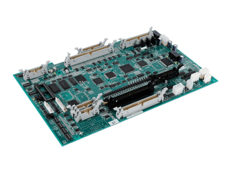
MCU Control Board Layout: Decoupling and Grounding Rules A microcontroller control board for a small appliance looks simple: an MCU, a few driver stages, a display, some buttons and a power supply. In practice it is one of the harder boards to get right, because the same board carries switching…

AI Smartphone PCB Design: Compute Density, Signals and Heat Smartphones stopped being simply “smart” once they began running inference locally. Adding a neural processing unit to an application processor changes far more than the bill of materials: it turns the main board into a compute platform where every square millimetre…
HDI Blind and Buried Via Process: Laser Drilling to Plating High-density interconnect boards fit more routing into less area, and the HDI blind and buried via process is what makes that density practical. A blind via connects an outer layer to an inner layer without passing through the whole board;…
PCB Circuit Board Design Steps: Requirements to Production Files A circuit board that works on the first prototype is not the product of a single clever decision. It is the result of a sequence of steps, each of which narrows the options available to the next. Skipping a step does…
PCB Design and Prototyping: Optimizing the Development Flow Prototyping is where a design stops being a drawing and starts producing data. The schedule risk in a hardware project is rarely in the schematic; it sits in the two or three weeks between finishing the layout and holding a working board,…
AI Server PCB Design: HDI, High-Speed Buses and Power The boards inside a training cluster are no longer oversized server motherboards. They are high-layer-count interconnect carriers whose job is to move hundreds of gigabytes per second between accelerators and to deliver several hundred watts to each of them without sagging.…
PCB Outline Design: Outline Layer, Panelization and Tolerances Most layout reviews spend their time on impedance and length matching and treat the board edge as a formality. The edge is what the fabricator machines first, what the assembler clamps, and what decides whether a thin product survives its own reflow…
AI Phone PCB Design: Stackup, Power and Thermal Paths A flagship handset is no longer a phone with a few smart features bolted on. It is a continuously running inference platform, and the board inside it has to carry camera streams, microphone arrays, an always-on vision pipeline and a cellular…
AI Computing Board Design: Five High-Performance Layout Challenges Accelerator cards and AI server compute trays have become the most demanding boards in mainstream electronics. A single package can present several hundred high-speed differential pairs, draw well over five hundred watts, and switch between idle and full load in microseconds. Once…
Automotive Chip PCB Layout: Placement, Power Decoupling, and EMC Guidelines Automotive control modules are built around a system-on-chip or a multi-die module that combines a processor, memory interfaces, and a set of high-speed serial links in a single package. The layout around that package decides whether the module survives the…