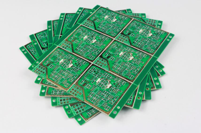
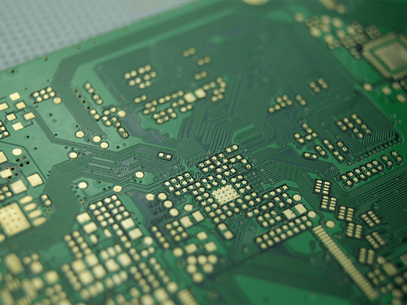
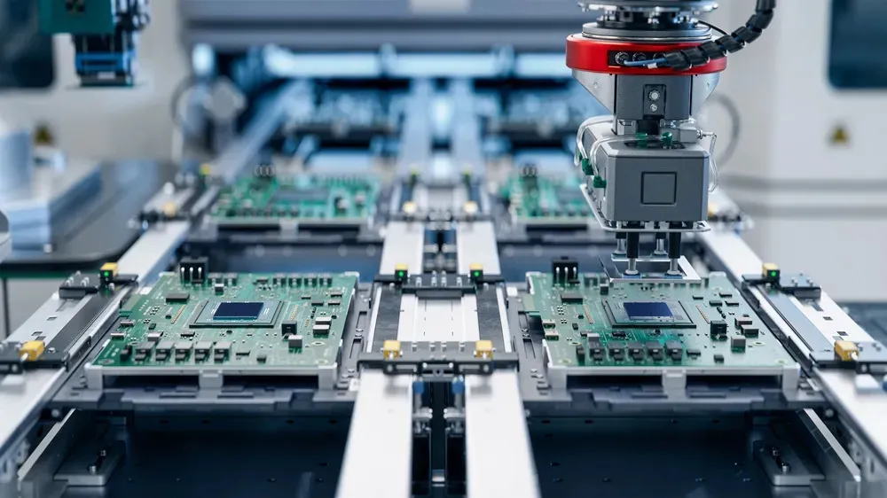
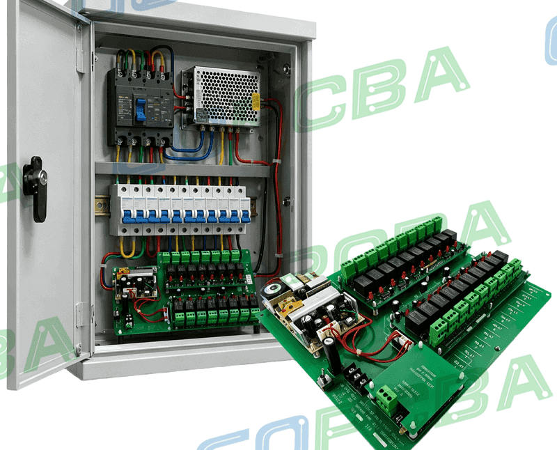
PCB Production Flow: From Design Files to Finished Board A finished circuit board is the output of two very different sequences: a design sequence that produces data, and a production sequence that turns that data into copper and laminate. The two meet at the manufacturing files. Understanding what happens after…
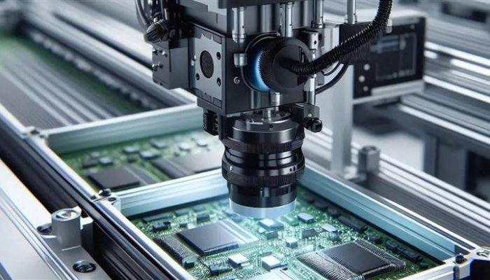
PCB Inspection After Fabrication: What to Check Once a board has been designed and built, the difference between a working assembly and a batch of scrap is measured at inspection. The checks are unglamorous, but each one maps to a specific failure mode that would otherwise be discovered by the…
Glass Fiber Board vs FR-4: Composition and Applications Ask for a glass fibre board and you may be handed something that belongs in a building, not in an electronic product. Ask for FR-4 and you will get the material that almost every rigid circuit board is made from. The two…
Flying Wires and Manual Placement in PCB Layout Autorouters have improved enormously, yet almost every professional layout still contains material that was placed and routed by hand. Part of that is judgement — a tool cannot know which return path matters — and part of it is the humble flying…
PCB Design Inputs and Steps: From Schematic to Gerber A board only turns out well if the people laying it out have the information they need, and most expensive respins trace back to something that was never supplied rather than to something the designer got wrong. The PCB design inputs…
High-Speed Multilayer PCB Design: Why More Layers Help When a design moves from tens of megahertz into the hundreds, the layer count stops being an accounting decision and becomes an electrical one. A two-layer board that worked at low speed develops reflections, crosstalk and radiated noise that no amount of…
Automotive ECU PCB Design: Mixed-Signal Layout and Reliability Walk into a modern vehicle and you are surrounded by dozens of hidden computers: airbag controllers, all-wheel-drive modules, GPS navigation, ADAS processors, infotainment, cameras, lidar and a cloud of small sensor nodes. Vehicle programmes routinely carry hundreds of electronic control units, and…
Photoresist Developing in PCB Fabrication: Control and Defects Imaging is the step where a design stops being data and becomes a pattern on copper foil, and photoresist developing is where that pattern first becomes visible. Everything that follows — etching, plating, line width, impedance — is built on the geometry…
High Reliability PCB Design: Thermal and Component Rules Boards that have to work in demanding environments are designed to a stricter set of rules than consumer products, and the difference is not one dramatic requirement but a large number of small ones applied consistently. The rules cover thermal placement, the…
Solder Mask Design: Openings, Dams and Thickness The solder mask is a thin polymer layer printed over the finished circuit, with openings only where a joint has to form. It is easy to treat as decoration, and doing so is expensive: the mask decides whether solder stays on the pad…