KingdaKingdaKingda

Call Us 24/7

+86-181-2376-9076

Send Us Mail

sales@gopcba.com

Our Location

Baoan District, Shenzhen, China

Language

  • enEnglish
    • fr France
    • itItalian
Kingda
  • Home
  • PCB Assembly
    • Prototype PCB Assembly
    • Turnkey PCB Assembly
    • Low Volume PCB Assembly
    • High Volume PCB Assembly
    • SMT PCB Assembly
    • Through-Hole PCB Assembly
    • Mixed Technology PCB Assembly
    • Flex PCB Assembly
  • Services
    • PCB Design/Layout
    • PCB Manufacturing
    • Rapid PCBA Prototyping
    • Components Procurement
    • Conformal Coating
    • PCBA Testing
    • Box Build Assembly
    • Wire & Cable Harness Assembly
  • Industry Solutions
    • Medical PCBA
    • Telecommunications PCBA
    • Energy PCBA
    • Industrial PCBA
    • Artificial Intelligence PCBA
    • IOT PCBA
  • Resources
    • PCB Capabilities
    • PCBA Capabilities
    • FAQ
    • Blog
  • About Us
    • About Us
    • Why Us
    • Quality Management
  • Contact Us
Get A Quote
5

Lead-Free Solder and Tin-Lead Assembly: What Changes

  • By Frank guo
  • 2026年 9月 13日
  • PCB Assembly
  • No Comments
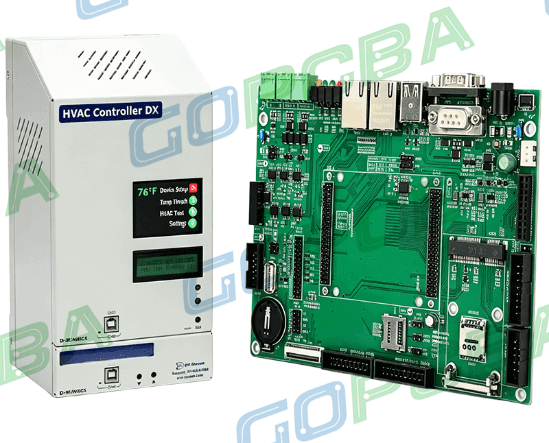
Lead-Free Solder and Tin-Lead Assembly: What Changes Assembly with tin-lead solder and assembly with lead-free solder look like the same process with a different alloy, and they are not. The alloy melts at a different temperature, which changes the entire thermal profile; the joints that form behave differently under stress;…
Continue Reading
HAVC Control System PCBA

Laminate Selection for High-Speed Designs: Performance Against Cost

  • By Frank guo
  • 2026年 9月 13日
  • PCB Assembly
  • No Comments
Laminate Selection for High-Speed Designs: Performance Against Cost The material a board is built on stops being a background choice once the data rates rise. Above roughly ten gigabits per second, a conventional laminate absorbs enough of the signal to consume the link budget on its own, and laminate selection…
Continue Reading
PCB Prototype Assembly

Calculating Trace Width for Current and Temperature Rise

  • By Frank guo
  • 2026年 9月 13日
  • PCB Assembly
  • No Comments
Calculating Trace Width for Current and Temperature Rise Trace width is decided by two questions that pull in opposite directions. The trace has to carry its current without getting too hot and without dropping too much voltage, which pushes the width up; and the routing has to fit into the…
Continue Reading
Applications_of_Automobile_PCB

Through-Hole Pad and Hole Size Design

  • By Frank guo
  • 2026年 9月 13日
  • PCB Assembly
  • No Comments
Through-Hole Pad and Hole Size Design Through-hole parts are easier to justify than to design. The decisions that matter are small numbers — the hole diameter, the land around it and the distance between two holes — and each of them is a compromise between making the part easy to…
Continue Reading
ptt_project

Reducing RF Effects in PCB Interconnect Design

  • By Frank guo
  • 2026年 9月 13日
  • PCB Assembly
  • No Comments
Reducing RF Effects in PCB Interconnect Design Once the signals on a board reach the gigahertz range, the interconnect stops behaving like a connection and starts behaving like a circuit. Corners reflect, surfaces resist more than their cross section suggests, finishes add loss where they were meant only to protect,…
Continue Reading
Outer-layer-UV-expose-and-etching8-1

Impedance Design on a Six-Layer Stack-Up

  • By Frank guo
  • 2026年 9月 13日
  • PCB Assembly
  • No Comments
Impedance Design on a Six-Layer Stack-Up A six-layer board is the point at which controlled impedance stops being optional and starts being structural. There are enough layers to give fast signals a proper reference, and enough density that the trace geometry which produces a given impedance has to be designed…
Continue Reading
Microsection of a multilayer board under a microscope

Power Plane Inset and the 20H Rule

  • By Frank guo
  • 2026年 9月 13日
  • PCB Assembly
  • No Comments
Power Plane Inset and the 20H Rule Open a well-designed multilayer board and the power plane is often slightly smaller than the plane above or below it. The difference is deliberate. It exists because the field between a plane pair is not entirely contained inside the board: at the cut…
Continue Reading
EV-Charger-PCBA

Black Hole Process and Electroless Copper Compared

  • By Frank guo
  • 2026年 9月 13日
  • PCB Assembly
  • No Comments
Black Hole Process and Electroless Copper Compared A drilled hole is not yet a connection. The wall of the hole is laminate, and laminate does not conduct, so before any copper can be electroplated onto it the surface has to be made conductive by some means. Two families of process…
Continue Reading
PCB Prototyping

Via Design Rules: Sizes, Spacing and Fanout

  • By Frank guo
  • 2026年 9月 13日
  • PCB Assembly
  • No Comments
Via Design Rules: Sizes, Spacing and Fanout Vias are the cheapest way to add a layer’s worth of routing, and they are also one of the largest single contributors to the cost of a board: the drilling and plating operations behind them account for a large share of what a…
Continue Reading
Industrial-5G-Networking-Equipment-PCBA

PCB Layout Workflow: From Schematic Review to Release

  • By Frank guo
  • 2026年 9月 13日
  • PCB Assembly
  • No Comments
PCB Layout Workflow: From Schematic Review to Release A layout does not become good because it was drawn carefully. It becomes good because the sequence of decisions was taken in an order that leaves each later decision with room to be made. The practical layout workflow below follows that order:…
Continue Reading
1 … 445 446 447 … 591

Search Posts

Categories

  • Electronic Materials
  • Electronical Engineering
  • Industrial Control
  • PCB Assembly
  • PCB Design
  • PCB Manufacturing

Recent Posts

Surface Mount Technology (SMT): Process, Components, Design Guidelines & PCB Assembly

Surface Mount Technology (SMT): Process, Components, Design Guidelines & PCB Assembly

Zane Zhang - 2026年 10月 2日
Cheap PCB Costs: PCB Design, PCB Manufacturing & SMT vs TH Guide

Cheap PCB Costs: PCB Design, PCB Manufacturing & SMT vs TH Guide

Jelly - 2026年 9月 30日
Cheap PCB Costs: PCB Design, PCB Manufacturing & SMT vs TH Guide

Cheap PCB Costs: PCB Design, PCB Manufacturing & SMT vs TH Guide

Jelly - 2026年 9月 30日

Tags

AOI inspection automotive electronics automotive PCBA quality automotive standards box build assembly component mounting component procurement component supplier conformal coating defect prevention DFM checks DFM review e-bom management electronic component shortage electronic manufacturing services electronic manufacturing standards Electronic Materials electronics design best practice electronics manufacturing capacity electronics sourcing high volume production industrial electronics insertion mount manufacturability review mass production quality mixed technology PCB PCBA inspection PCBA prototype PCBA turnkey PCBA volume pricing PCB Design PCB layout rules PCB Manufacturing PCB sourcing power electronics PCB printed circuit board prototype quick turn PCB reflow soldering SMT assembly quality SMT production solder paste inspection solder paste printing surface mount technology vehicle electronics wave soldering
GOPCBA-logo

As a professional China PCB assembly manufacturer, we provide a full range of electronic manufacturing services from PCB fabrication, PCBA to OEM/ODM, including PCB design, PCB layout, rapid PCBA prototyping, components procurement, SMT/ THT assembly, china pcb assembly, china pcb prototype, PCBA testing and box build assembly.

Linkedin Facebook-f X-twitter Youtube Instagram

PCB ASSEMBLY

  • Prototype PCB Assembly
  • Low Volume PCB Assembly
  • High Volume PCB Assembly
  • Turnkey PCB Assembly
  • SMT PCB Assembly
  • Through-Hole PCB Assembly
  • Mixed Technology PCB Assembly
  • Flex PCB Assembly

OUR SERVICES

  • PCB Design/Layout
  • PCB Manufacturing
  • Rapid PCBA Prototyping
  • Components Procurement
  • Conformal Coating
  • PCBA Testing
  • Box Build Assembly
  • Wire & Cable Harness Assembly

TECHNICAL SUPPORT

  • About Us
  • Quality Management
  • Artificial Intelligence PCBA
  • Industrial PCBA
  • IOT PCBA
  • Medical PCBA
  • Energy PCBA
  • Telecommunications PCBA

Copyright © 2026. Shenzhen Kingda Electronics Co., LTD  All rights reserved. 

  • Sitemap
  • Terms of Service
  • Privacy Policy
Zmdi Zmdi-email Phone-square Whatsapp Weixin
x

ABOUT US

Progressively maintain extensive infomediaries via extensible nich. Capitalize on low hanging fruit. a ballpark value added is activity to beta test. Override the digital divide with additional click throughs from fruit.

LOCATIONS

map

New York Office

+07 554 332 322
contact@example.com
office@example.com
37 San Fairport, NY 14450, New York City
All Locations

FOLLOW US