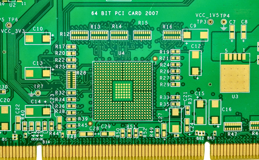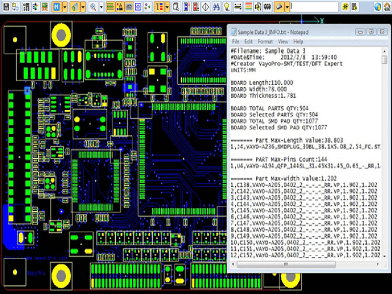
Thermal Management in High-Speed PCB Design Heat in a fast board comes from more places than the obvious ones. The large devices dominate, but the transmission lines themselves dissipate energy, and at high rates that loss is not negligible. Thermal management is therefore part of the layout rather than a…
Length Matching Rules for DDR Routing: Groups and Tolerance A parallel memory bus depends on several signals arriving together. The controller launches data, a strobe edge tells the device when to sample, and the margin between them is the window in which the whole bus works or fails. Trace length…
Layer Assignment in Multilayer Boards: Power, Ground and Signal Layer assignment is the part of multilayer design that is hardest to change later. Once the stack-up is fixed, the impedance of every controlled trace is fixed with it, the reference plane each signal returns through is decided, and the space…
Flex PCB Design: Materials, Bend Radius and Support A flex PCB is designed against a different set of constraints from a rigid board, and the difference is mechanical as much as electrical. The board has to bend without breaking, the conductors in the bend region have to survive repeated movement,…
Half-Bridge Converter Layout: Power, Gate Drive and Ground A half-bridge converter is a switching power stage, and its layout decides whether the efficiency calculated on paper survives contact with the board. The currents are large, the edges are fast, and the same node that carries the main power also carries…
Replacing Via in Pad With an Ordinary Via: When It Pays A via placed inside a component pad is one of the more expensive features a board can carry, and it is often specified for good reasons. It shortens the path from a ball or a land to the layer…
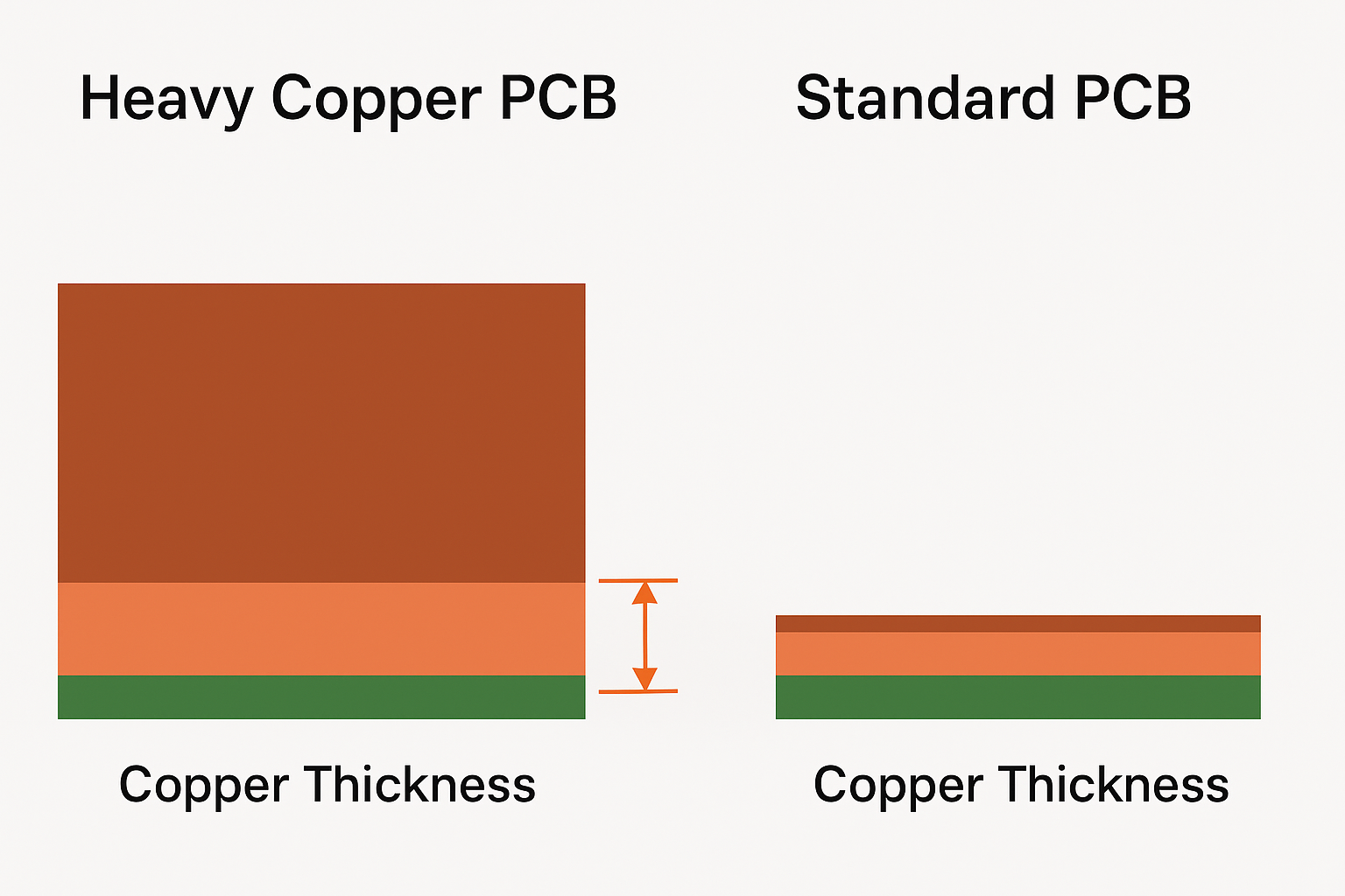
Heavy Copper in HDI Boards: Compatibility and Design Rules Two directions in board technology pull against each other. High density interconnect pushes toward thin dielectrics, small vias and fine traces, because that is how more connections fit into less area. Heavy copper pushes toward thick conductors and wider features, because…
PCB Warpage: Causes, Consequences and Controls A board that is flat when it leaves the fabricator is not necessarily flat when it reaches the assembly line. Warpage develops across the whole life of a panel — during pressing, while solder mask and legend are cured, through the thermal shock of…
Routing Priority and Crosstalk Control in PCB Layout Routing that begins before the board has been thought about produces work that has to be undone. The usual sequence is familiar: power and general signals are routed first, and somewhere in the middle of the board a group of high-speed nets…
HDI Layout: Shrinkage Compensation and Microvia Rules High density interconnect changes the questions a layout has to answer. On a conventional board the constraint is usually space: how to fit the routing into the area available. On an HDI board the constraint becomes agreement — between the stack-up and the…