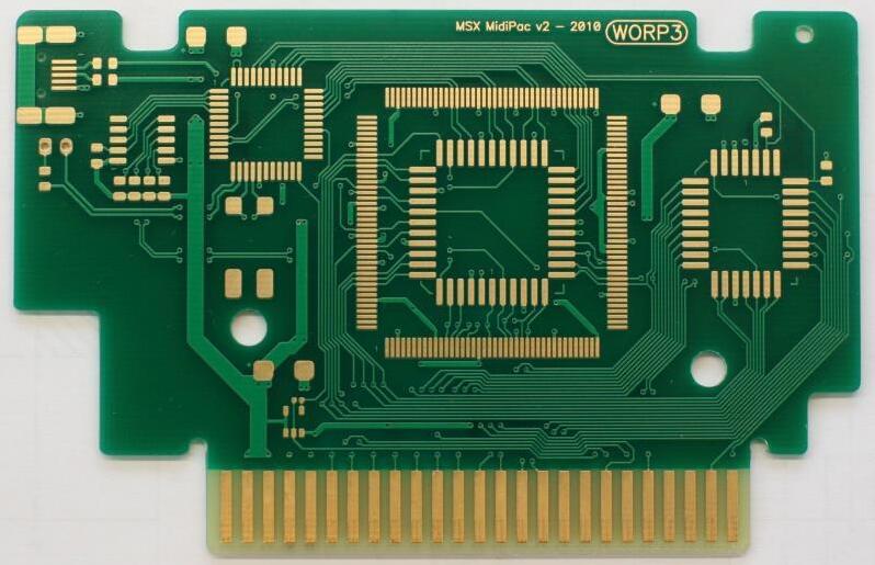
PCB EMI Shielding

PCB EMI Shielding: Nested Shielding, Grounding and Shielding Can Design Guide

During product development, cost, schedule, quality, and electrical performance are closely connected. From these perspectives, it is generally more effective to address PCB EMI Shielding and electromagnetic compatibility (EMC) requirements as early as possible in the design cycle. Adding shielding components or implementing quick fixes late in development can increase…
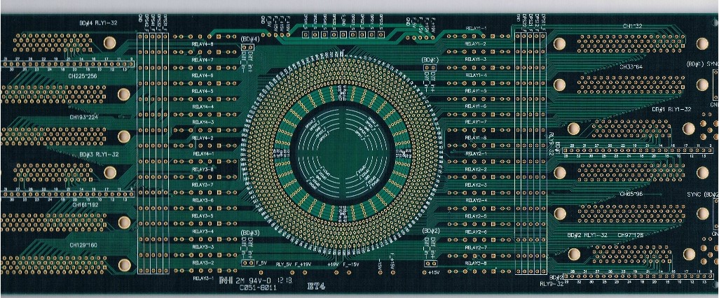
PCB Trace Width

PCB Trace Width and Current Capacity: Power, Thermal and Via Design Guide

Not every PCB requires strict control of trace width and current capacity. However, when a circuit carries high current, experiences transient current pulses, or contains high-power components, conductor dimensions become critical design parameters. In motor-control systems, power electronics, industrial equipment, automotive electronics, battery systems, and other high-power applications, PCB traces…
PCB Design Guidelines

PCB Design Guidelines: Manufacturing Rules for Trace Width, Spacing and V-Cut

PCB design is closely related to manufacturing capability. A circuit board may be electrically functional in theory but still require design changes if its trace width, spacing, hole size, copper clearance, or mechanical features exceed the manufacturer’s process capability. For this reason, designers should consider PCB Design Guidelines and Design…
PCB Substrate Materials

PCB Substrate Materials: Key Material Properties for High-Speed PCB Design

The electrical, mechanical, and thermal behavior of a printed circuit board depends heavily on the materials used in its construction. In addition to copper conductors and electronic components, the selection of PCB Substrate Materials has a direct impact on signal integrity, thermal management, mechanical reliability, and long-term performance. For conventional…
Cadence PCB Design

Cadence PCB Design: High-Speed PCB Layout, Routing and Signal Integrity Guide

Cadence is a widely used electronic design automation (EDA) platform that supports many stages of electronic product development, including ASIC design, FPGA development, and printed circuit board design. For complex and high-speed electronic products, Cadence PCB Design provides an integrated environment for schematic capture, component and footprint development, PCB layout,…
High-Speed PCB Design

Signal Integrity in High-Speed PCB Design: Challenges, Control Methods and Best Practices

As digital systems continue to increase in processing speed and data bandwidth, Signal Integrity has become a critical consideration in modern electronic hardware design. Wireless base stations, network controllers, wired communication infrastructure, high-performance computing platforms, industrial systems, aerospace electronics, and other advanced equipment increasingly rely on high-speed interfaces to transfer…
Multilayer Circuit Board

Multilayer PCB Applications: Key Industries, Benefits and Manufacturing Considerations

Printed circuit boards have been widely used in electronic equipment for decades. As electronic products continue to become smaller, faster, and more highly integrated, conventional single-sided and double-sided boards are increasingly limited by available routing space and electrical performance requirements. The development of the Multilayer PCB has provided an effective…
Copper Clad Laminate

China Copper Clad Laminate (CCL) Industry: Future Materials, High-Performance CCL and IC Substrate Trends

The development of the electronics industry continues to drive demand for higher-performance substrate materials. As electronic products become smaller, faster, more integrated, and more energy-efficient, traditional materials are increasingly being challenged by requirements for high-frequency transmission, thermal management, reliability, and environmental compliance. As a fundamental material used in printed circuit…
182

High-Frequency PCB Power Noise: Causes, Coupling Mechanisms and Suppression Methods

Power noise is one of the most important sources of interference in high-speed and high-frequency electronic systems. As switching frequencies increase and PCB feature sizes become smaller, even relatively small parasitic inductance, capacitance, and resistance can affect system performance. In a High-Frequency PCB, power distribution is not simply a method…