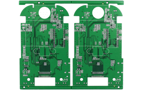
Portable life-monitoring equipment such as ECG, SpO₂, temperature, and respiration monitors places demanding requirements on PCB design. Physiological signals can be only millivolt- or microvolt-level at the sensing interface, making them highly susceptible to interference from digital switching, power conversion, wireless communication, and external electromagnetic fields. For these applications, a…
In the development of portable life-monitoring equipment, one of the most common engineering challenges is preventing wireless communication circuits from interfering with low-level physiological signal acquisition. Bluetooth and Wi-Fi modules generate high-frequency RF energy during transmission. If the RF energy couples into sensitive ECG, SpO₂, or other analog acquisition circuits,…
Medical electronics place higher demands on PCB performance than many conventional electronic products. In addition to electrical functionality, a Medical PCB must consider reliability, manufacturability, traceability, cleanliness, and long-term stability. These requirements become particularly important in patient monitoring and life-monitoring equipment, where unstable electrical performance can affect the accuracy of…
Medical monitoring equipment places demanding requirements on PCB reliability, especially when the electronic system is used for long-term physiological signal acquisition or operates near the human body. A 4-layer PCB may pass functional testing immediately after assembly while still containing latent material, contamination, insulation, or interconnection risks that only become…
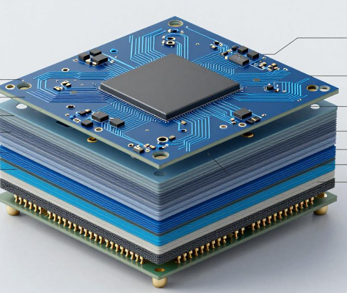
In the total cost structure of a multilayer PCB, prepreg (PP) can represent a significant portion of the raw-material cost, particularly for high-layer-count, large-format, and high-volume production. The selection of PP materials and the overall stackup directly affect material utilization, lamination performance, dielectric thickness, impedance, and production cost. Many hardware…
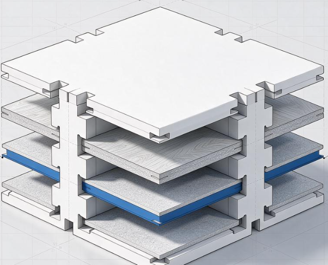
In high-volume multilayer PCB production, stacking multiple sheets of prepreg (PP) is a common method for achieving a specific dielectric thickness. When no single PP construction matches the target thickness, engineers may combine two or more sheets to build the required dielectric layer. Although this approach can provide flexibility during…
When engineers calculate dielectric thickness in a multilayer PCB stackup, the primary focus is often target impedance. However, the physical topography created by etched inner-layer copper is equally important. After inner-layer etching, copper-covered areas and resin-filled areas do not have the same surface height. During lamination, the resin in prepreg…
Many recurring PCB production redesigns are not caused by manufacturing equipment failures or process problems. In many cases, the underlying issue can be traced back to insufficient PCB DFM review during the prototype stage. Engineers often focus on whether a prototype functions correctly, whether the board powers on successfully, and…
In PCB manufacturing, prototype development is often accompanied by multiple rounds of design optimization. Engineers may adjust component placement, routing, layer stackup, impedance parameters, hole dimensions, materials, or manufacturing processes after each prototype build. These changes are normal during product development. The real risk occurs when updated design files, manufacturing…
In high-speed multilayer PCB design, engineers often rely on the dielectric constant (Dk) provided in a laminate datasheet when calculating controlled impedance. The problem is that a Dk value measured at a low frequency cannot always accurately represent the electrical behavior of the same material at hundreds of megahertz or…